Pinholes and bubbles on SMT solder joints are common welding defects in PCB production, which directly reduce solder joint reliability, cause hidden issues like cold solder and poor conductivity, and even lead to product failure. The root causes mostly lie in two core links: solder paste selection/control and stencil printing process, rather than a single operational error. This article sorts out key fault points and quick troubleshooting methods to help factories locate problems efficiently and solve solder joint pinhole and bubble issues.
1. Solder Paste: Source Control to Avoid Gas Residue
The composition and storage state of solder paste directly determine gas generation during welding, being the fundamental cause of pinholes and bubbles. Focus on 3 checkpoints:
- Excessive volatile content: Prioritize solder paste marked with low voidage and low VOCs. Never use ordinary solder paste for high-precision fine-pitch processes to reduce gas generation during melting.
- Moisture absorption and deterioration: Store solder paste hermetically at 2-8℃. Return to room temperature for 4-6 hours (unseal never) before use and finish within 24 hours after unsealing. Moisture-absorbed solder paste will form bubbles due to water vapor during welding.
- Mismatched powder size and stencil: Use Type 4/5 fine-powder solder paste for 01005/0201 micro-components and Type 3 for regular components. Large-powder solder paste for fine-pitch printing is prone to air entrapment, directly causing pinholes.
2. Printing Process: Core Control to Eliminate Air Entrapment & Paste Residue
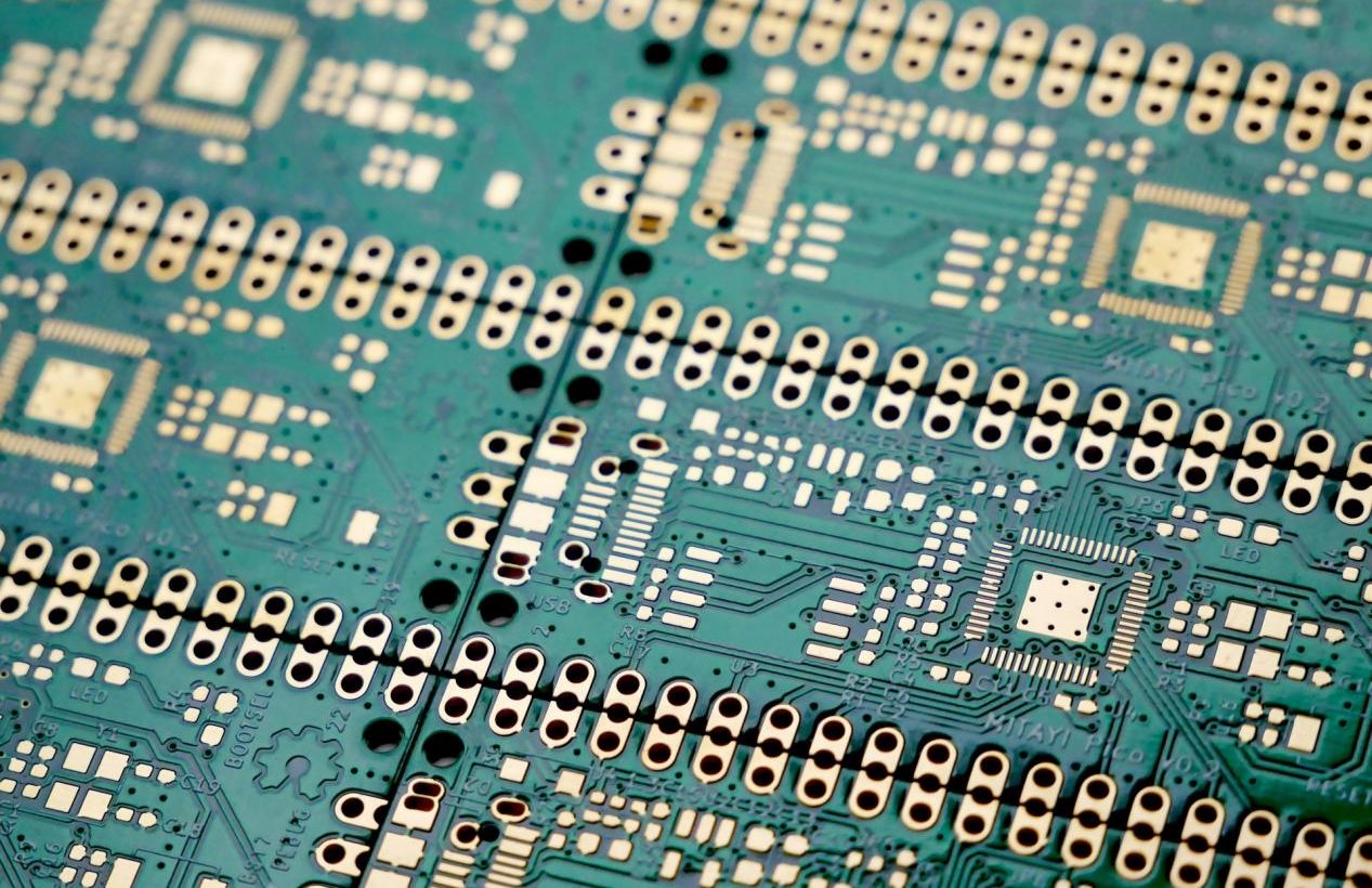
Stencil printing is the main link of solder paste air entrapment. Irrational process parameters, poor stencil design and inadequate cleaning will cause air to be wrapped in solder paste, forming defects after welding. Key 4 checkpoints:
- Unreasonable stencil design: Add exhaust grooves to stencil apertures for fine-pitch/large-area pads; control aperture aspect ratio at 1:1~1.5:1 and area ratio ≥0.66. Imbalanced ratios or no exhaust grooves lead to air entrapment. Polish stencil aperture burrs immediately to avoid uneven coating from paste scratching.
- Abnormal printing parameters: Optimal scraper pressure 0.3-0.8MPa and printing speed 20-50mm/s. Excessive pressure or overhigh speed forces solder paste to extrude and trap air. Adopt stage separation speed for stencil: 1-3mm/s for fine-pitch areas to prevent paste lifting and air hole formation.
- Abnormal solder paste rolling: Keep paste roll diameter 10-20mm during printing to ensure uniform filling into stencil apertures. Insufficient, agglomerated paste or narrow rolling range causes uneven coating and air entrapment.
- Inadequate stencil cleaning: Wipe stencil with dry-wet-dry method every 5-10 boards printed; clean ultrasonically with special cleaner after production. Paste residue in apertures causes repeated air entrapment and solder joint defects in subsequent printing.
3. Overlooked Link: PCB Pre-Treatment Before Printing
PCB pad cleanliness and flatness are key auxiliary factors, easily ignored but indirectly causing pinholes and bubbles:
- Oil, dust and oxide layers on pads affect solder paste wettability, and gaps in oxide layers trap air. Clean pads with plasma or alcohol before printing; rework severely oxidized ones directly.
- Control PCB warpage ≤0.75% and fix with support pins during printing. Warpage creates gaps between stencil and pads, allowing air into solder paste and forming bubbles finally.
4. On-Site Quick Troubleshooting Process
For sudden solder joint pinholes and bubbles in production, follow these steps to locate problems quickly and reduce downtime losses:
- Prioritize trial printing with new batch of qualified solder paste to rule out source issues like moisture absorption and deterioration.
- Check stencil apertures for blockage and residue; conduct small-batch trial production after adjusting scraper pressure/separation speed.
- Randomly inspect PCB pad cleanliness and flatness; clean and fix unqualified products.
- If all above are normal, properly extend reflow preheating time by 10-20s to fully discharge volatiles in solder paste.
Conclusion
The core solution to SMT solder joint pinholes and bubbles is to control gas generation from the solder paste source, eliminate solder paste air entrapment from the printing process, and control details of PCB pre-treatment simultaneously. Without complex equipment, standardizing solder paste usage procedures, calibrating printing parameters and cleaning stencils regularly can significantly reduce such defect rates and improve SMT solder joint reliability and production yield.