Before using the smt pick and place machine for PCB placement, we can understand how the PCB is designed and processed
Today we will talk about the solder mask and how it is designed
What is a solder mask?
How do you maintain the best condition of your PCB? You need to avoid rust, oxidation can cause rust. This is easy to do with solder mask.
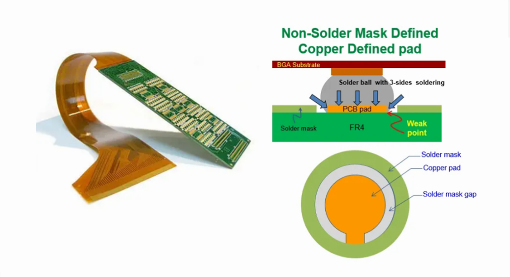
We also refer to solder mask as solder mask or solder mask. It is the thin layer that masks the copper traces. You don’t need to solder on the printed circuit boards (PCBs) on both sides. It is simpler to ensure the robustness and high functionality of the PCB. We use resin as the main material for the solder mask. It works well in insulation, moisture resistance, high temperature resistance and solder resistance.
The PCB is green, which is the color of the solder mask green oil. However, with us, you can also get soldermask in other colors. Choose from options in white, black, blue, yellow, red, and more. Adding color can add a little personality. That’s why more and more OEM manufacturers are picking colors for themselves. This is how they know it’s their board.
In addition, OEM manufacturers select colors by market segment. For example, people in the artificial intelligence profession now choose red. You use the chalkboard for projects that require more light reflection. This is very easy to find the board.
According to your needs, we use different colors. It is also possible that the same circuit board includes different colors of solder mask.
Solder Mask: Top Features
Solder masks are increasingly prevalent. People also focus on power and volume.
Solder mask prevents solder bridges from occurring in masked areas. Reflow soldering is an important part of SMT assembly. It enables electronic components to be mounted on circuit boards through solder paste.
In addition, it can hinder the formation of solder bridges. These can be created quickly or otherwise between carefully packed pads.
If you don’t apply solder mask, the copper traces will stick to the solder paste. This happens with many hand-assembled circuits. In turn, it may lead to short courses. This affects functionality and robustness. Soldermask also protects copper traces from corrosion, oxidation, and grime.
That’s why most mass-produced PCBs have it. You can’t take risks!
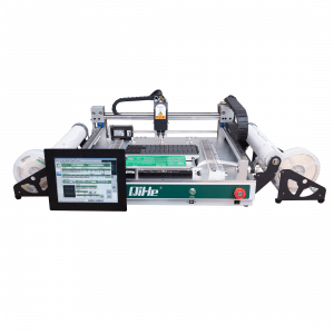
Qihe smt pick and place machine TVM802a
The Four Primary Types of Solder Mask
Solder mask prevents conductive solder bridging between various electronic components. Essentially, it thwarts short circuits. The different PCB solder mask layers are as follows.
a. Top and bottom masks: Electronic engineers are aware of various openings. He knows what is added through ink, epoxy or thin film technology. He was then able to solder the component pins on the board with the help of the confirmed orientation. You can also notice the pattern of conductive traces on the top of the board. You call these top stalking. The lower one is the bottom mask.
b. Epoxy Liquids: If you want an inexpensive option, choose an epoxy liquid. Thermoset polymers have a variety of applications. Silkscreen is a printing technique. It uses a woven mesh to support the ink-blocking pattern. The grid creates an open area for ink transfer. Heat curing is part of the final cleaning process.
c. Liquid inks are photoimageable: We supply solder mask as ink formulation. You can spray ink into the PCB. Then you can expose the schema and develop it. It is important to note that we use this process as well as liquid ink formulations. This requires a clean environment free of contaminants and particles. People were able to remove it after exposing it to UV light. I do this through a high pressure water spray called developer.
d. The dry film is photoimageable: apply this solder mask by means of vacuum lamination. Once developed, you can create openings and solder parts to copper pads. Also, use tin to protect copper circuits. Then we remove the dry film.
Solder mask manufacturing process
The fabrication of solder mask involves several stages. We need accuracy. Does it fit the manufacturing experience and technology?
Step 1: Clean the circuit board: Clean the surface of the circuit board. Remove dirt and keep the surface dry together.
Step 2: Ink Application: The second step is to load the clean cardboard into the vertical coater. With elements such as reliability requirements, we can see the coating thickness. When solder mask ink is present on different board sections, the width may vary.
Step 3: Pre-hardening: Pre-hardening is not the same as full-hardening. Stabilize the coating on the board. This way, unneeded layers are removed from the board during the development phase.
Step 4: Imaging and Hardening: Mount the clear film on the plate. Combine it with the circuit drawing and then expose it to UV light. The process was developed to partially mask the solder mask with a transparent film. The slicing film is masked with circuit drawings – stick to pre-hardening. Ensure proper alignment when hardening. Otherwise, it can hinder the exposure of the copper foil. The vulnerability affects functionality or short-circuits.
Step 5: Development: At the next level, you place the PCB in developer to clean any unwanted solder mask. This ensures that the desired copper foil is exposed.
Step 6: Final Hardening and Cleaning: In a later step, you will need to perform a final hardening. I do this so that the solder mask ink can be installed on the surface of the PCB. You will need to clean these boards before further processing. We do it in the form of assembly or surface finish.
you can choose a reflow oven to meets your need like qfr630,qrf835,qrf1235
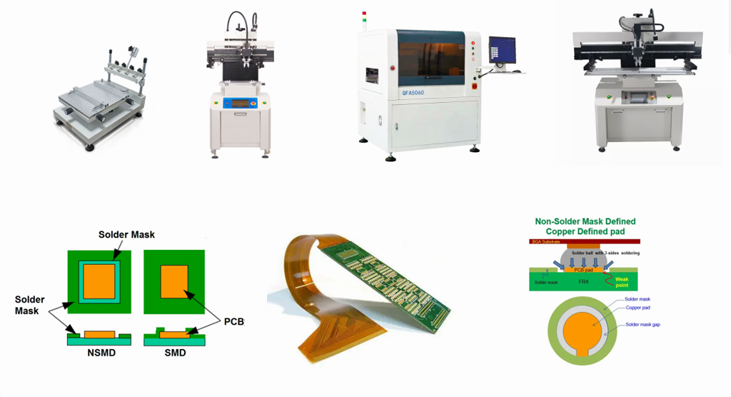
stencil printer model qh3040,qp3250,qfa5060
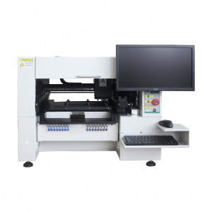
Also we have different kinds of smt pick and place machine like tvm802a,tvm802b,tvm802ax,tvm802bx,tvm925s,tvm926s,ql41,qm61,qm62,qm81,qm10
Qihe smt pick and place machine catalog
-
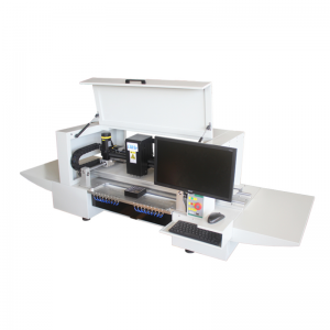
 SMT semi-automatic pick and place machine with Dispenser
 -
TVM925 SMT pick and place machine 4 head 38 feeders slots assembly of electronic components
-
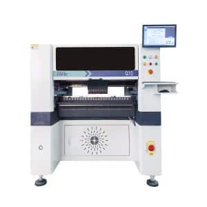
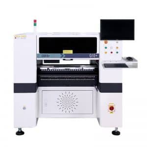
Q10 SMT Automatic pick and place machine 10 Heads 100 Slots High Precision and High Efficiency SMT/LED Assembly
-
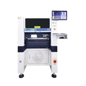
Q6 SMT pick and place machine 6heads 50slots With PCB Rail Servo Pick&Place Machine
-
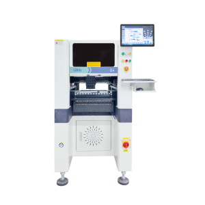
Q4 SMT pick and place machine 4heads 50slots With PCB Rail Servo Pick&Place Machine
-
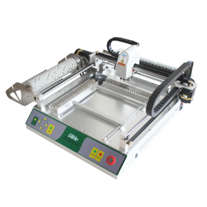
TVM802B Plus SMT pick and place machine 2heads 58slots desktop pick&place deluxe edition
-
QM10 SMT pick and place machine 10heads 80slots Fully Automatic Chip mounter SMT Assembly
-
TVM802BX SMT pick and place machine 2heads 46slots desktop pnp mounter deluxe edition
-
QL41 SMT pick and place machine 4heads 8slots LED for 1.2meters led strip pick&place machine
FAQ about smt pick and place machine
WHAT IS SMT ASSEMBLY LINE?
With the development of technology, future electronic products will be lighter, smaller and thinner. Traditional assembly technology can no longer meet the requirements of high-precision and high-density assembly. A new type of PCB assembly technology-SMT (Surface Mount Technology) has emerged. SMT Assembly is the use of automated machines to assemble electronic components on the surface of the circuit board. Its density, high speed, standardization and other characteristics occupies an absolute advantage in the field of circuit assembly technology. In addition, SMT assembly has a wide range of uses.
WHAT IS SMT pick and place machine?
SMT (Surface Mounted Technology) is a comprehensive system engineering technology, which covers substrates, design, equipment, components, assembly processes, production accessories and management. When it comes to SMT pick and place machines, the automatic SMT production line requires automatic loading and unloading machine, automatic solder paste printing machine, placement machine, reflow soldering machine, AOI inspection equipment, connecting table, etc. For these SMT assembly line equipment, Qihe SMT can offer you machines in prototype SMT line, small SMT production line, mass production SMT line at low SMT line cost. Contact us now if you are interested.
WHAT IS SMT PROCESS?
There are mainly three steps in SMT assembly line process flow: solder paste printing, components placement and reflow soldering.
- Solder Paste Printing
Its function in SMT line process is to print the solder-free paste on the pads of the PCB to prepare for the soldering of the components. The equipment used is a screen printing machine, located at the forefront of the SMT production line.
- Components Placement
Its function is to accurately install the surface mount components on the fixed position of the PCB. The equipment used is a placement machine, located behind the screen printing machine in the SMT production line.
- Reflow Soldering
Its function in SMT manufacturing line is to melt the solder paste so that the surface mount components and the PCB board are firmly bonded together. The equipment used is a reflow oven, located behind the placement machine in the fully automatic SMT production line.