What should be paid attention while designing a single chip microcomputer control board ?The most basic process of designing a circuit board can be divided into three major steps: the design of the circuit schematic diagram, the generation of the netlist, and the design of the printed circuit board. Whether it is the device layout or wiring on the board, there are specific requirements.Together discuss with qihe smt equipment editor today.
The most basic process of designing a circuit board can be divided into three major steps: the design of the circuit schematic diagram, the generation of the netlist, and the design of the printed circuit board. Whether it is the device layout or wiring on the board, there are specific requirements.
What is single chip microcomputer?
This is a microcomputer built using separate components (CPU, Memory, etc.). For some specific applications, we also have single chip computers in a VLSI chip. This single chip microcomputer will have a CPU, memory and I/O interfaces, timers, ADC/DACs etc. on a single chip itself.
How to design a microprocessor?
The Microprocessor Chip: Design Guidelines, Functionality …
These steps are as follows:
Ascertain the capabilities the new processor will have or need to have.
Provide a layout of the datapath to manage the needed capabilities.
Delineate the machine code instruction format or instruction set architecture (ISA).
Build the necessary logic to control the datapath.
For example, parallel input and output lines should be avoided as much as possible to avoid interference. The parallel routing of two signal lines should be separated by ground wires, and the wiring of two adjacent layers should be perpendicular to each other as much as possible. Parasitic coupling is easy to occur in parallel. The power and ground wires should be divided into two layers perpendicular to each other as much as possible. In terms of line width, a wide ground wire can be used to make a loop for digital circuit PCBs, that is, to form a ground network (analog circuits cannot be used in this way), and a large area of copper is laid.
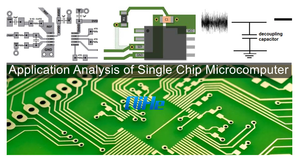
The following article explains the principles and some details that need to be paid attention to in the design of the microcontroller control board.
Component layout
In terms of component layout, the components related to each other should be placed as close as possible. For example, clock generators, crystal oscillators, and clock input terminals of the CPU are prone to noise, and they should be placed closer. For those devices that are prone to noise, small current circuits, high current circuit switching circuits, etc., try to keep them away from the logic control circuit and storage circuit (ROM, RAM) of the microcontroller. If possible, these circuits can be made into circuits board, which is conducive to anti-interference and improves the reliability of circuit work.
Decoupling capacitor
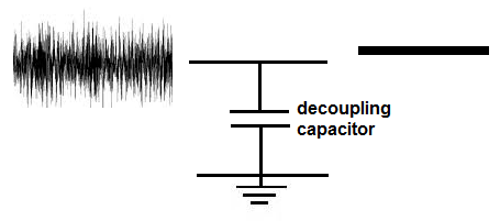
Try to install decoupling capacitors next to key components, such as ROM, RAM and other chips. In fact, printed circuit board traces, pin connections, and wiring may all contain large inductance effects. Large inductance can cause severe switching noise spikes on the Vcc trace. The only way to prevent switching noise spikes on the Vcc trace is to place a 0.1uF electronic decoupling capacitor between VCC and power ground. If surface mount components are used on the circuit board, chip capacitors can be used directly against the components and fixed on the Vcc pin. It is best to use ceramic capacitors because they have low electrostatic loss (ESL) and high-frequency impedance, and the dielectric stability of this capacitor over temperature and time is also very good. Try not to use tantalum capacitors because of their high impedance at high frequencies.
What is the rule of placing for decoupling capacitor?
·Connect an electrolytic capacitor of about 100uF across the power input terminal of the printed circuit board. If the volume allows, a larger capacitance is better.
·In principle, a 0.01uF ceramic chip capacitor needs to be placed next to each integrated circuit chip. If the gap of the circuit board is too small to fit, a 1~10 tantalum capacitor can be placed around every 10 chips.
· For components with weak anti-interference ability and large current changes when they are turned off, and storage components such as RAM and ROM, a decoupling capacitor should be connected between the power line (Vcc) and the ground line.
·The lead wire of the capacitor should not be too long, especially the high frequency bypass capacitor should not have a lead wire.
Ground design
In the single-chip microcomputer control system, there are many types of ground wires, including system ground, shielding ground, logic ground, analog ground, etc. Whether the ground wire layout is reasonable will determine the anti-interference ability of the circuit board. When designing ground wires and grounding points, the following issues should be considered:
·Logic ground and analog ground should be wired separately and cannot be used together. Connect their respective ground wires to the corresponding power ground wires. When designing, the analog ground wire should be as thick as possible, and the grounding area of the lead-out terminal should be increased as much as possible. Generally speaking, for the input and output analog signals, it is best to isolate them from the microcontroller circuit through optocouplers.
·When designing the printed circuit board of the logic circuit, its ground wire should form a closed-loop form to improve the anti-interference ability of the circuit.
·The ground wire should be as thick as possible. If the ground wire is very thin, the resistance of the ground wire will be large, causing the ground potential to change with the change of the current, causing the signal level to be unstable, and resulting in a decrease in the anti-interference ability of the circuit. If the wiring space allows, ensure that the width of the main ground wire is at least 2~3mm, and the ground wire on the component pin should be about 1.5mm.
· Pay attention to the selection of the grounding point. When the signal frequency on the circuit board is lower than 1MHz, since the electromagnetic induction between the wiring and the components has little influence, and the circulating current formed by the grounding circuit has a greater influence on the interference, it is necessary to use a little grounding so that it does not form a loop. When the signal frequency on the circuit board is higher than 10MHz, due to the obvious inductance effect of the wiring, the impedance of the ground wire becomes very large. At this time, the circulating current formed by the ground circuit is no longer the main problem. Therefore, multi-point grounding should be adopted to minimize the ground impedance.
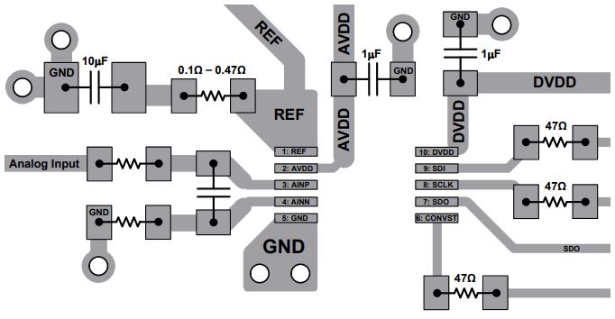
Power line layout
In addition to the layout of the power line, the width of the line should be as thick as possible according to the magnitude of the current. When wiring, the line direction of the power line and the ground line should be consistent with the line shape of the data line. At the end of the wiring work, use the ground These methods help to enhance the anti-interference ability of the circuit.
·The width of the data line should be as wide as possible to reduce the impedance. The width of the data line is at least not less than 0.3mm (12mil), and it is more ideal to use 0.46~0.5mm (18mil~20mil).
·Because a via hole on the circuit board will bring a capacitive effect of about 10pF, which will introduce too much interference for high-frequency circuits, so the number of via holes should be reduced as much as possible when wiring. Furthermore, too many via holes will also reduce the mechanical strength of the circuit board.
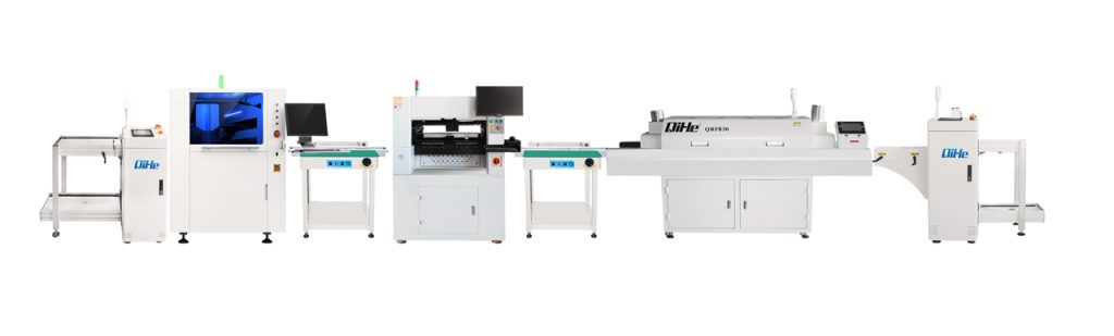
Best seller SMT Machine :Qihe smt line products
-
 SMT semi-automatic pick and place machine with Dispenser
 -
TVM925 SMT pick and place machine 4 head 38 feeders slots assembly of electronic components
-
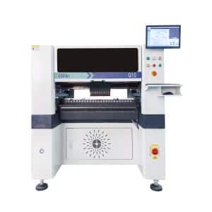
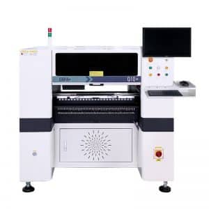
Q10 SMT Automatic pick and place machine 10 Heads 100 Slots High Precision and High Efficiency SMT/LED Assembly
-
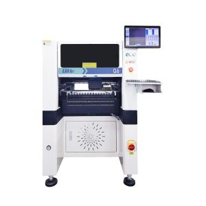
Q6 SMT pick and place machine 6heads 50slots With PCB Rail Servo Pick&Place Machine
-
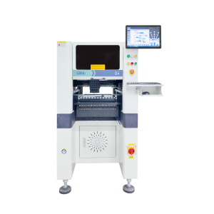
Q4 SMT pick and place machine 4heads 50slots With PCB Rail Servo Pick&Place Machine
-
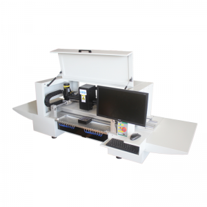
TVM802B Plus SMT pick and place machine 2heads 58slots desktop pick&place deluxe edition
-
QM10 SMT pick and place machine 10heads 80slots Fully Automatic Chip mounter SMT Assembly
-
TVM802BX SMT pick and place machine 2heads 46slots desktop pnp mounter deluxe edition
-
QL41 SMT pick and place machine 4heads 8slots LED for 1.2meters led strip pick&place machine
Smt equipment line video
What is SMT in engineering?
Surface mount technology is a part of the electronic assembly that deals with the mounting of electronic components to the surface of a PCB. Electronic components mounted this way are called surface-mounted devices (SMD). SMT was developed to minimize manufacturing costs while making efficient use of board space.Qihe SMT company develops and produces all kinds of SMT equipment suitable for world wide market, including pnp machine,reflow oven,stencil printer,pcb handling machines,and other products.
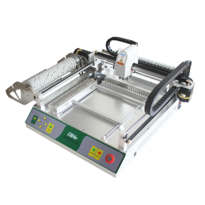
Small desktop pick and place machine TVM802A,TVM802B,TVM802AX,TVM802BX series suitable for beginners, for hobbiest or low vol usag,low cost smt pick and place machine.
Advanced level 4-head LED strip placement QL41 led machines and with rail universal series TVM925S,TVM926S,
Fully automatic 6-10-head placement QM61,QM62,QM81,QM10,machines, which are suitable for high volume mass production in factories.
Know more about us https://www.qhsmt.com/about-qihe-smt-equipment/
Follow us on social media https://www.facebook.com/Qihesmt/
What is SMT in programming?
Offline Automated Programming vs Inline SMT Programming
Qihe pick and place machine can be programmed directly on the SMT equipment .
Or Coordinates can also be imported csv file through programming software.
Currently supported software such as protel,DXP,Altium Designer,Pads,Candes,proteus,DXP.
Inline SMT programming is a solution to consider for narrow segments of device programming requiring short programming times, with medium to high volume, for just one device type.
WHAT IS SMT pick and place machine?
SMT (Surface Mounted Technology) is a comprehensive system engineering technology, which covers substrates, design, equipment, components, assembly processes, production accessories and management. When it comes to SMT pick and place machines, the automatic SMT production line requires automatic loading and unloading machine, automatic solder paste printing machine, placement machine, reflow soldering machine, AOI inspection equipment, conveyor,connecting table, etc. For these SMT assembly line equipment, Qihe SMT can offer you machines in prototype SMT line, small SMT production line, mass production SMT line at low SMT line cost. Contact us now if you are interested.
How to choose the right smt pick and place robot?
SMT Pick and place robots can execute virtually all smd material handling operations both cost-efficiently and effectively — With several designs and configurations available in the market, it can be challenging to pick one that suits your operational needs. To help you make the right decision, some factors and features you should look out for when purchasing a pick and place robot.The most important thing is the operating system, then the hardware configuration, the types of components supported, and the speed of operation, the accuracy of placement, and the smt setup cost of the entire smt line .
Qihe smt pick&place machine is a professional operating system independently developed. It has more than ten years of user experience, combined with the algorithm improvement of world-renowned colleges, and the most advanced flying camera and motion system. It is your best choice. The system is friendly for beginners and professionals.
WHAT IS SMT ASSEMBLY LINE?
With the development of technology, future electronic products will be lighter, smaller and thinner. Traditional assembly technology can no longer meet the requirements of high-precision and high-density assembly. A new type of PCB assembly technology-SMT (Surface Mount Technology) has emerged. SMT Assembly is the use of automated machines to assemble electronic components on the surface of the circuit board. Its density, high speed, standardization and other characteristics occupies an absolute advantage in the field of circuit assembly technology. In addition, SMT assembly has a wide range of uses.
https://www.qhsmt.com/fully-automatic-smt-pick-and-place-machine-line/
smt equipment