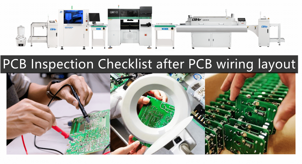
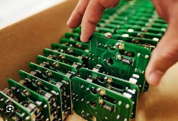
Inspection after PCB wiring is also necessary, so how to check the wiring in PCB design to pave the way for later design? Some designs have many different requirements, and a PCB inspection checklist can help you keep track of everything that needs to be checked.Today author from QiHe smt pick and place machine discussing about it with you .
General PCB design drawing inspection items
1) Has the circuit been analyzed? Has the circuit been divided into basic units for smooth signal?
2) Does the circuit allow short or isolated critical leads?
3) Are the places that must be shielded effectively shielded?
4) Have you made full use of the basic grid graphics?
5) Is the size of the printed circuit board the optimal size?
6) Is the selected wire width and spacing used as much as possible?
7) Has the preferred pad size and hole size been used?
8) Are the photographic plates and sketches appropriate?
9) Is there a minimum of jumper wires used? Do jumper wires go through components and accessories?
l0) Are the letters visible after assembly? Are they the correct size and type?
11) In order to prevent foaming, has the large area of copper foil been opened?
12) Is there a tool positioning hole?
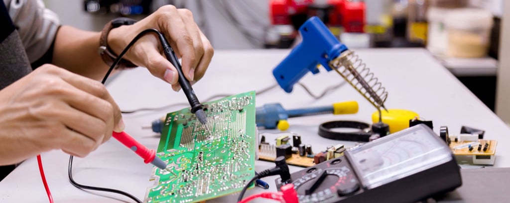
PCB electrical characteristics inspection items
1) Have you analyzed the influence of wire resistance, inductance, and capacitance? Especially have you analyzed the influence of the key voltage drop phase to ground?
2) Do the spacing and shape of the wire accessories meet the insulation requirements?
3) Is the insulation resistance value controlled and specified at key points?
4) Is the polarity adequately identified?
5) Have you measured the effect of wire spacing on leakage resistance and voltage from a geometric point of view?
6) Has the medium used to change the surface coating been identified?
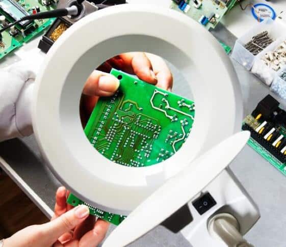
PCB physical characteristics inspection items
1) Are all pads and their positions suitable for final assembly?
2) Can the assembled printed circuit board meet the shock and vibration conditions?
3) What is the spacing of the specified standard components?
4) Are loosely mounted components or heavy parts secured?
5) Is the heat dissipation and cooling of the heating element correct? Or is it isolated from the printed circuit board and other heat-sensitive components?
6) Are the voltage dividers and other multi-lead components positioned correctly?
7) Are the components arranged and oriented for easy inspection?
8) Are all possible interferences eliminated on the printed circuit board and on the entire printed circuit board assembly?
9) Is the size of the positioning hole correct?
10) Are the tolerances complete and reasonable?
11) Are the physical properties of all coatings controlled and signed off?
12) Is the hole to lead diameter ratio within an acceptable range?
PCB Mechanical Design Factors
Although a printed circuit board supports components mechanically, it cannot be used as a structural member of the entire device. At the edge of the printing plate, a certain amount of support should be carried out at least every 5 inches. The factors that must be considered in the selection and design of printed circuit boards are as follows;
1) The structure of the printed circuit board – size and shape.
2) Types of mechanical accessories and plugs (seats) required.
3) Adaptability of the circuit to other circuits and environmental conditions.
4) Depending on factors such as heat and dust, consider installing the PCB vertically or horizontally.
5) Some environmental factors that require special attention, such as heat dissipation, ventilation, shock, vibration, and humidity. Dust, salt spray and radiation.
6) The degree of support.
7) Hold and fix.
8) Easy to take off.
PCB printed circuit board installation requirements
It should be supported at least within 1 inch of all three edges of the printed circuit board. According to practical experience, the spacing between the supporting points of printed circuit boards with a thickness of 0.031–0.062 inches should be at least 4 inches; for printed circuit boards with a thickness greater than 0.093 inches, the spacing of supporting points should be at least 5 inches. Taking this measure can increase the rigidity of the printed circuit board and destroy possible resonance of the printed circuit board.
A certain type of printed circuit board usually needs to consider the following factors before deciding on the mounting technology they use.
1) The size and shape of the printed circuit board.
2) The number of input and output terminals.
3) Available equipment space.
4) Desired ease of loading and unloading.
5) Type of mounting accessories.
6) Required heat dissipation.
7) Shieldability required.
8) The type of circuit and the relationship with other circuits.
Dial-out requirements for printed circuit boards
1) Printed circuit board area that does not require mounting components.
2) The influence of plugging tools on the installation distance between two printed circuit boards.
3) Specially prepare mounting holes and slots in the printed circuit board design.
4) When the plug-in tool is to be used in the equipment, especially its size should be considered.
5) A plug-in device is required, which is usually permanently fixed to the printed circuit board assembly with rivets.
6) In the mounting frame of the printed circuit board, a special design such as a load bearing flange is required.
7) The adaptability of the plugging tool used to the size, shape and thickness of the printed circuit board.
8) The cost involved in using the plug-in tool includes both the price of the tool and the increased expenditure.
9) In order to fasten and use plugging tools, it is required to have access to the interior of the equipment to a certain extent.
PCB Mechanical Considerations
The substrate properties that have a significant impact on printed circuit assemblies are: water absorption, coefficient of thermal expansion, heat resistance, flexural strength, impact strength, tensile strength, shear strength, and hardness.
All of these characteristics affect both the functionality of the printed circuit board structure and the productivity of the printed circuit board structure.
For most applications, the dielectric substrate for printed wiring boards is one of the following substrates:
1) Phenolic impregnated paper.
2) Acrylic-polyester impregnated randomly arranged glass mat.
3) Epoxy impregnated paper.
4) Epoxy impregnated glass cloth.
Each substrate can be flame retardant or combustible. Above-mentioned 1,2,3 can be punched. The most commonly used material for metallized hole printed circuit boards is epoxy-glass cloth, its dimensional stability is suitable for high-density circuit use, and it can minimize the occurrence of cracks in metallized holes.
One disadvantage of epoxy-glass cloth laminates is that they are difficult to punch in the usual thickness range for printed circuit boards. For this reason, all holes are usually drilled and profile milled to form the shape of the printed circuit board.
PCB Electrical Considerations
In DC or low-frequency AC applications, the most important electrical properties of insulating substrates are: insulation resistance, electrical isolation resistance, printed wire resistance, and breakdown strength.
In high frequency and microwave occasions, it is: dielectric constant, capacitance, and dissipation factors.
In all applications, however, the current carrying capacity of the printed conductors is important.
Read more: PCB Inspection Checklist after PCB wiring layoutBest seller SMT Machine :Qihe smt line products
-
 SMT semi-automatic pick and place machine with Dispenser
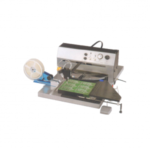
 -
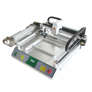
TVM925 SMT pick and place machine 4 head 38 feeders slots assembly of electronic components
-
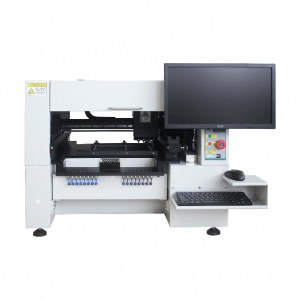
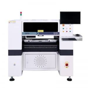
Q10 SMT Automatic pick and place machine 10 Heads 100 Slots High Precision and High Efficiency SMT/LED Assembly
-
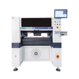
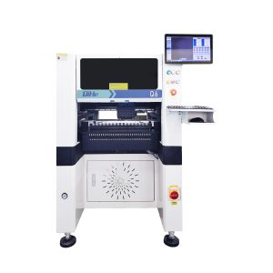
Q6 SMT pick and place machine 6heads 50slots With PCB Rail Servo Pick&Place Machine
-
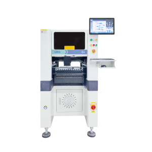
Q4 SMT pick and place machine 4heads 50slots With PCB Rail Servo Pick&Place Machine
-
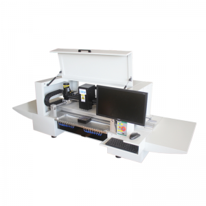
TVM802B Plus SMT pick and place machine 2heads 58slots desktop pick&place deluxe edition
-
QM10 SMT pick and place machine 10heads 80slots Fully Automatic Chip mounter SMT Assembly
-
TVM802BX SMT pick and place machine 2heads 46slots desktop pnp mounter deluxe edition
-
QL41 SMT pick and place machine 4heads 8slots LED for 1.2meters led strip pick&place machine
What is SMT in engineering?
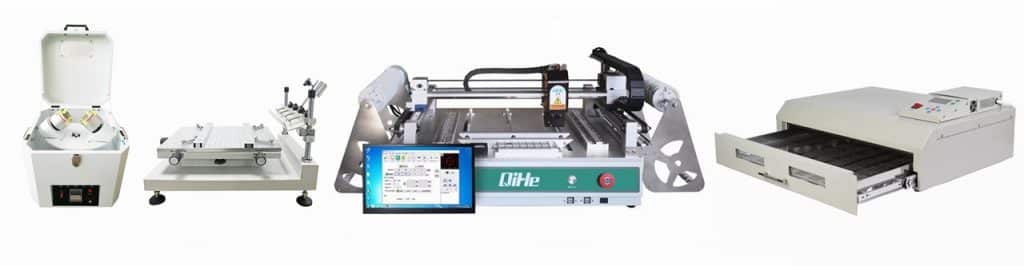
Surface mount technology is a part of the electronic assembly that deals with the mounting of electronic components to the surface of a PCB. Electronic components mounted this way are called surface-mounted devices (SMD). SMT was developed to minimize manufacturing costs while making efficient use of board space.Qihe SMT company develops and produces all kinds of SMT equipment suitable for world wide market, including pnp machine,reflow oven,stencil printer,pcb handling machines,and other products.
Small desktop pick and place machine TVM802A,TVM802B,TVM802AX,TVM802BX series suitable for beginners, for hobbiest or low vol usag.
Advanced level 4-head LED strip placement QL41 led machines and with rail universal series TVM925S,TVM926S,
Fully automatic 6-10-head placement QM61,QM62,QM81,QM10,machines, which are suitable for high volume mass production in factories.
Know more about us https://www.qhsmt.com/about-qihe-smt-equipment/
Follow us on social media https://www.facebook.com/Qihesmt/
What is SMT in programming?
Offline Automated Programming vs Inline SMT Programming
Qihe pick and place machine can be programmed directly on the SMT equipment .
Or Coordinates can also be imported csv file through programming software.
Currently supported software such as protel,DXP,Altium Designer,Pads,Candes,proteus,DXP.
Inline SMT programming is a solution to consider for narrow segments of device programming requiring short programming times, with medium to high volume, for just one device type.
WHAT IS SMT pick and place machine?
SMT (Surface Mounted Technology) is a comprehensive system engineering technology, which covers substrates, design, equipment, components, assembly processes, production accessories and management. When it comes to SMT pick and place machines, the automatic SMT production line requires automatic loading and unloading machine, automatic solder paste printing machine, placement machine, reflow soldering machine, AOI inspection equipment, conveyor,connecting table, etc. For these SMT assembly line equipment, Qihe SMT can offer you machines in prototype SMT line, small SMT production line, mass production SMT line at low SMT line cost. Contact us now if you are interested.
WHAT IS SMT ASSEMBLY LINE?
With the development of technology, future electronic products will be lighter, smaller and thinner. Traditional assembly technology can no longer meet the requirements of high-precision and high-density assembly. A new type of PCB assembly technology-SMT (Surface Mount Technology) has emerged. SMT Assembly is the use of automated machines to assemble electronic components on the surface of the circuit board. Its density, high speed, standardization and other characteristics occupies an absolute advantage in the field of circuit assembly technology. In addition, SMT assembly has a wide range of uses.
https://www.qhsmt.com/fully-automatic-smt-pick-and-place-machine-line/