For many years, people have always believed that the fewer board layers, the lower the cost, but there are many other factors that affect the manufacturing cost of the board. In recent years, the cost difference between multilayer boards has been greatly reduced. It is better to start the design with more circuit layers and distribute the copper evenly to avoid being forced to add new layers only to find that a small number of signals do not meet the defined rules and space requirements near the end of the design. Careful planning before design will save a lot of trouble in wiring. In PCB layout design, there is a complete set of methods for improving the layout rate. Here,qihe smt pick and place machine sharing you with effective techniques to improve the PCB design layout rate and design efficiency, which can not only save the project development cycle for customers, but also maximize Guarantee the quality of the finished product to the maximum extent.
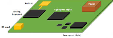
Board size and wiring layers need to be determined early in the design. If the design calls for the use of high-density ball grid array (BGA) components, the minimum number of routing layers required to route these devices must be considered. The number of wiring layers and the way of stacking (stack-up) will directly affect the wiring and impedance of the printed lines. The size of the board helps determine the stackup and trace width to achieve the desired design effect.
The autorouter itself doesn’t know what to do. To accomplish the routing task, the routing tool needs to work within the correct rules and constraints. Different signal lines have different wiring requirements, and all signal lines with special requirements must be classified, and different design classifications are also different. Each signal class should have a priority, the higher the priority, the stricter the rules. Rules related to trace width, maximum number of vias, parallelism, interaction between signal lines, and layer constraints have a great impact on the performance of routing tools. Careful consideration of design requirements is an important step in successful routing.
To optimize the assembly process, design for manufacturability (DFM) rules impose constraints on component layout. If the assembly department allows components to move, the circuit can be properly optimized for easier automated routing. The defined rules and constraints affect the layout design.
The routing channel and via area need to be considered during layout. These paths and areas are obvious to the designer, but the automatic routing tool will only consider one signal at a time. By setting the routing constraints and setting the layer of the routing signal line, the routing tool can be as the designer imagined. That completes the wiring.
In the fan-out design phase, to allow the auto-routing tool to connect the component pins, each pin of the surface mount device should have at least one via, so that the board can be routed to the inner layer when more connections are required. Connectivity, In-Circuit Test (ICT) and Circuit Reprocessing.
In order to maximize the efficiency of the automatic routing tool, it is necessary to use the largest via size and printed line possible, and the spacing is set to 50mil, which is ideal. Use the via type that maximizes the number of routing paths. When performing fan-out design, it is necessary to take into account the problem of circuit in-circuit testing. Test fixtures can be expensive and are usually ordered close to full production when it is too late to consider adding nodes to achieve 100% testability.
After careful consideration and prediction, the design of circuit online test can be carried out at the early stage of design and realized in the later stage of the production process. The fan-out type of the via is determined according to the wiring path and circuit online test. Power and ground will also affect the wiring and fan-out design. . In order to reduce the inductance generated by the connection line of the filter capacitor, the via hole should be as close as possible to the pin of the surface mount device. If necessary, manual wiring can be used, which may affect the original wiring path, and may even cause you to reinstall Considering which vias to use, it is therefore necessary to consider the relationship between vias and lead inductance and prioritize via specifications.
Although this article focuses on automatic routing issues, manual routing is and will continue to be an important process in printed circuit board design. Use manual routing to help the automatic routing tool to complete the routing work. Regardless of the number of critical signals, route these signals first, either manually or in conjunction with automated routing tools. Critical signals usually require careful circuit design to achieve desired performance. After the wiring is completed, the relevant engineering personnel will check the signal wiring. This process is much easier. Once the checks pass, fix the wires and start autorouting the rest of the signals.
The wiring of key signals needs to consider controlling some electrical parameters during wiring, such as reducing distributed inductance and EMC, and the wiring of other signals is similar. All EDA vendors provide a way to control these parameters. After understanding the input parameters of the automatic routing tool and the influence of the input parameters on the routing, the quality of the automatic routing can be guaranteed to a certain extent.
Signals should be automatically routed using common rules. By setting restrictions and forbidden routing areas to limit the layers used by a given signal and the number of vias used, the routing tool can automatically route according to the engineer’s design ideas. If there is no limit to the number of layers used by the autorouting tool and the number of vias placed, every layer will be used during autorouting, and many vias will be generated.
After setting the constraints and applying the rules created, the autorouting will achieve something close to what you expect, although some housekeeping may be required, as well as securing room for other signals and nets to be routed. After a part of the design is completed, fix it to prevent it from being affected by the subsequent wiring process.
Use the same procedure to route the rest of the signals. The number of routings depends on the complexity of the circuit and how many general rules you define. After each type of signal is completed, the constraints on the rest of the net routing are reduced. But with that comes a lot of signal routing that requires manual intervention. The current automatic routing tools are very powerful and can usually complete 100% routing. However, when the automatic routing tool does not complete all the signal routing, the remaining signals need to be manually routed.
If the EDA tool software you use can list the routing length of the signal, check the data, and you may find that some signal routing with few constraints are very long. This problem is relatively easy to deal with, and the signal routing length can be shortened and the number of vias can be reduced through manual editing. During the finishing process, you need to determine which wiring is reasonable and which wiring is not reasonable. Like manual routing design, automatic routing design can also be organized and edited during the inspection process.
Read more: How to Design a PCB Layout: A Comprehensive GuideBest seller SMT Machine :Qihe smt line products
-
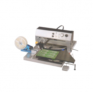
 SMT semi-automatic pick and place machine with Dispenser
 -
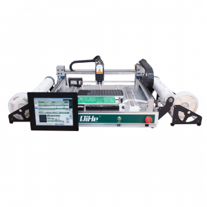
TVM925 SMT pick and place machine 4 head 38 feeders slots assembly of electronic components
-
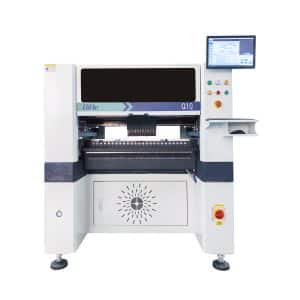
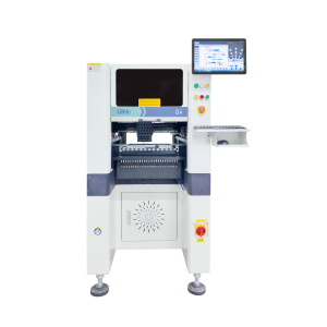
Q10 SMT Automatic pick and place machine 10 Heads 100 Slots High Precision and High Efficiency SMT/LED Assembly
-
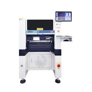
Q6 SMT pick and place machine 6heads 50slots With PCB Rail Servo Pick&Place Machine
-
Q4 SMT pick and place machine 4heads 50slots With PCB Rail Servo Pick&Place Machine
-
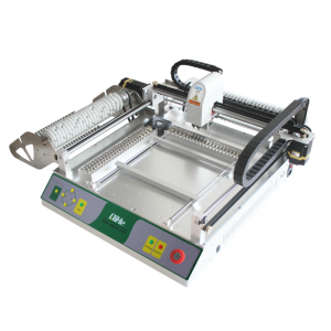
TVM802B Plus SMT pick and place machine 2heads 58slots desktop pick&place deluxe edition
-
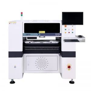
QM10 SMT pick and place machine 10heads 80slots Fully Automatic Chip mounter SMT Assembly
-
TVM802BX SMT pick and place machine 2heads 46slots desktop pnp mounter deluxe edition
-
QL41 SMT pick and place machine 4heads 8slots LED for 1.2meters led strip pick&place machine
What is SMT in engineering?
Surface mount technology is a part of the electronic assembly that deals with the mounting of electronic components to the surface of a PCB. Electronic components mounted this way are called surface-mounted devices (SMD). SMT was developed to minimize manufacturing costs while making efficient use of board space.Qihe SMT company develops and produces all kinds of SMT equipment suitable for world wide market, including pnp machine,reflow oven,stencil printer,pcb handling machines,and other products.
Small desktop pick and place machine TVM802A,TVM802B,TVM802AX,TVM802BX series suitable for beginners, for hobbiest or low vol usag.
Advanced level 4-head LED strip placement QL41 led machines and with rail universal series TVM925S,TVM926S,
Fully automatic 6-10-head placement QM61,QM62,QM81,QM10,machines, which are suitable for high volume mass production in factories.
Know more about us https://www.qhsmt.com/about-qihe-smt-equipment/
Follow us on social media https://www.facebook.com/Qihesmt/
What is SMT in programming?
Offline Automated Programming vs Inline SMT Programming
Qihe pick and place machine can be programmed directly on the SMT equipment .
Or Coordinates can also be imported csv file through programming software.
Currently supported software such as protel,DXP,Altium Designer,Pads,Candes,proteus,DXP.
Inline SMT programming is a solution to consider for narrow segments of device programming requiring short programming times, with medium to high volume, for just one device type.
WHAT IS SMT pick and place machine?
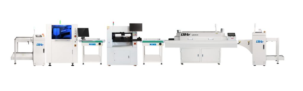
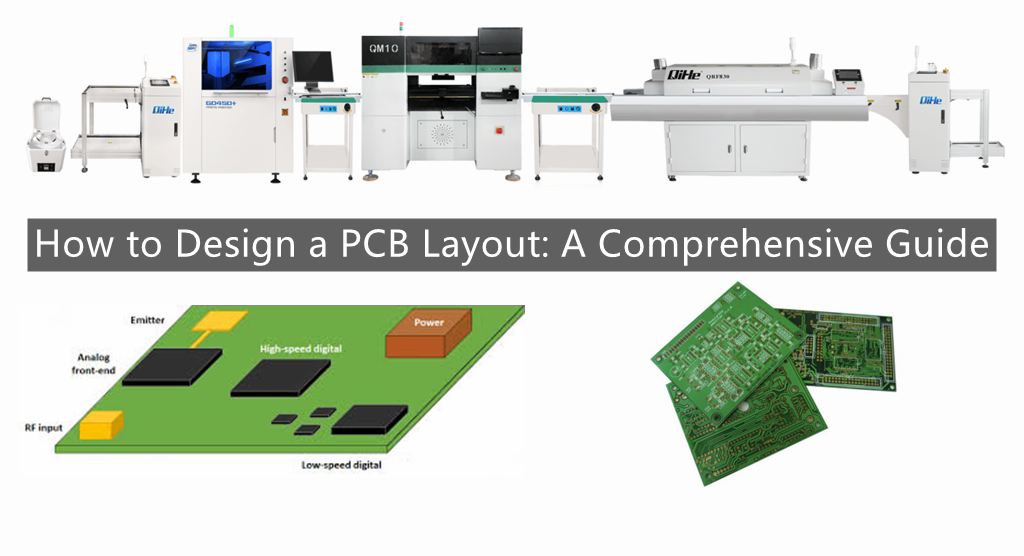
SMT (Surface Mounted Technology) is a comprehensive system engineering technology, which covers substrates, design, equipment, components, assembly processes, production accessories and management. When it comes to SMT pick and place machines, the automatic SMT production line requires automatic loading and unloading machine, automatic solder paste printing machine, placement machine, reflow soldering machine, AOI inspection equipment, conveyor,connecting table, etc. For these SMT assembly line equipment, Qihe SMT can offer you machines in prototype SMT line, small SMT production line, mass production SMT line at low SMT line cost. Contact us now if you are interested.
WHAT IS SMT ASSEMBLY LINE?
With the development of technology, future electronic products will be lighter, smaller and thinner. Traditional assembly technology can no longer meet the requirements of high-precision and high-density assembly. A new type of PCB assembly technology-SMT (Surface Mount Technology) has emerged. SMT Assembly is the use of automated machines to assemble electronic components on the surface of the circuit board. Its density, high speed, standardization and other characteristics occupies an absolute advantage in the field of circuit assembly technology. In addition, SMT assembly has a wide range of uses.
https://www.qhsmt.com/fully-automatic-smt-pick-and-place-machine-line/