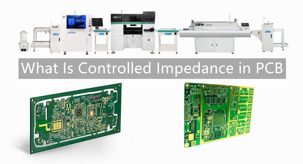
PCBs have the unique job of carrying electric signals between connecting parts. These electronic signals are necessary for a device to perform its function, and it won’t work without them. These signals travel through signal traces that run through the PCB. However, they don’t do so freely, as it takes time for them to travel along these transmission lines. That time delay can increase or decrease depending on several factors, such as materials. Controlled impedance is about controlling the resistance that a signal trace puts on a signal.Today qihe smt pick and place machine sharing what is controlled impedance in PCB.
Resistance
When an alternating current flows through a conductor, the resistance it encounters is called Impedance, which is Z and the unit is Ω. The resistance at this time is different from the resistance encountered by DC current. In addition to the resistance of resistance, there are also resistance problems of inductive reactance (XL) and capacitive reactance (XC).
To distinguish the resistance of direct current, the resistance encountered by alternating current is called impedance (Z).
Z=√ R2 + (XL-XC)2
Impedance (Z)
In recent years, with the improvement and application of IC integration, the frequency and speed of signal transmission are getting higher and higher. Therefore, in the printed board wire, when the signal transmission (transmission) reaches a certain value, it will be affected by the printed board wire itself. , resulting in severe distortion or complete loss of the transmitted signal. This shows that the “thing” that “flows” through the PCB wires is not current, but the transmission of square wave signals or pulses in energy.
Characteristic impedance control (Z0)
The resistance encountered when the above-mentioned “signal” is transmitted is also called “characteristic impedance”, and the representative symbol is Z0. Therefore, it is not enough to solve the problems of “on”, “off” and “short circuit” on the PCB wire, but also to control the characteristic impedance of the wire. That is to say, the transmission lines for high-speed transmission and high-frequency signal transmission are much stricter in quality than transmission wires. No longer is the “open circuit/short circuit” test passed, or the gap or burr does not exceed 20% of the line width, it can be accepted. It must be required to measure the characteristic impedance value, and this impedance must also be controlled within the tolerance, otherwise, it will only be scrapped and not reworked.
Signal Propagation and Transmission Lines
Definition of signal transmission line
According to the principle of electromagnetic waves, the shorter the wavelength (λ), the higher the frequency (f). The product of the two is the speed of light. That is C= λ.f =3×1010 cm/s
Although any component has a high signal transmission frequency, after being transmitted through the PCB wire, the original high transmission frequency will be reduced, or the time will be delayed. Therefore, the shorter the wire length, the better.
It is beneficial to increase the PCB wiring density or shorten the wire size. However, as the frequency of the component increases or the pulse period shortens, the length of the wire approaches a certain range of the signal wavelength (speed). At this time, when the component is transmitted on the PCB wire, there will be obvious “distortion”.
3.4.4 of IPC-2141 proposes: When the signal is transmitted in the wire, if the length of the wire is close to 1/7 of the signal wavelength, the wire at this time is regarded as a signal transmission line.
Transmission rate and dielectric constant
Signal transmission speed of different boards at 30MHZ
Dielectric material Tg ( °C ) Dielectric constant Signal transmission speed (m/?s)
Vacuum / 1.0 300.00
PTFE / 2.2 202.26
Thermosetting polypropyl ether 210 2.5 189.74
Cyanate resin 225 3.0 173.21
PTFE resin + E glass cloth / 2.6 186.25
Cyanate resin + glass cloth 225 3.7 155.96
Polyimide + glass cloth 230 4.5 141.42
Quartz / 3.9 151.98
Epoxy glass cloth 130±5 4.7 138.38
Aluminum / 9.0 100.00
It can be seen from the above table that as the dielectric constant (εr) increases, the transmission speed of the signal in the dielectric material decreases. To obtain a high signal transmission speed, a high characteristic impedance value is required; for a high characteristic impedance, a low dielectric constant (εr) material must be selected; the dielectric constant (εr) of polytetrafluoroethylene (TeflON) is the smallest, and the transmission fastest.
FR-4 sheet is composed of epoxy resin and E-grade glass cloth, with a dielectric constant (εr) of 4.7. The signal transmission speed is 138m/μs. Changing the resin system can easily change the dielectric constant (εr).
Reason for characteristic impedance value control
When the electronic equipment (computer, communication machine) is in operation, the signal sent by the driver element (Driver) will reach the receiver element (Receiver) through the PCB transmission line. When the signal is transmitted in the signal line of the printed board, its characteristic impedance value Z0 must match the “electronic impedance” of the head and tail components, so that the “energy” in the signal can be completely transmitted.
Once the quality of the printed board is poor and Z0 exceeds the tolerance, the transmitted signal will have problems such as Reflection, Dissipation, Attenuation, or Delay. In severe cases, the wrong signal will be transmitted and the machine will crash.
Only by strictly selecting boards and controlling the production process can Z0 on multi-layer boards meet the specifications required by customers. The higher the electronic impedance of the component, the faster its transmission speed, so the Z0 of the PCB must be increased accordingly to meet the requirements of matching components. Z0 qualified multi-layer boards can be regarded as qualified products required by high-speed or high-frequency signals.
Relationship between characteristic impedance ZO and sheet material and process
The characteristic impedance Z0 calculation formula of the microstrip line structure: Z0 = 87/r +1.41 ln5.98H / (0.8W+T)
Among them: εr-dielectric constant H-dielectric thickness W-conductor width T-conductor thickness The lower the εr of the plate, the easier it is to increase the Z0 value of the PCB circuit, and match the output impedance value of the high-speed component.
The characteristic impedance Z0 is inversely proportional to the εr of the plate
Z0 increases with increasing media thickness. Therefore, for high-frequency lines with strict Z0, strict requirements are put forward for the error of the dielectric thickness of the copper-clad laminate base material. Typically, the media thickness should not vary by more than 10%.
Effect of medium thickness on characteristic impedance Z0
As the wiring density increases, the increase in dielectric thickness will cause signal transmission lines for high-frequency lines and high-speed digital lines. With the increase in conductor wiring density, the dielectric thickness should be reduced to eliminate or reduce noise caused by electromagnetic interference. Signal or crosstalk problems, or greatly reduce εr, choose low εr substrate.
According to the characteristic impedance Z0 calculation formula of the microstrip line structure: Z0 = 87/r +1.41 ln5.98H / (0.8W+T)
Copper foil thickness (T) is an important factor affecting Z0, the thicker the wire, the smaller its Z0. But its range of variation is relatively small.
The effect of wire width on characteristic impedance Z0
Z0 increases rapidly as the line width W becomes narrower, so to control Z0, the line width must be strictly controlled. At present, the signal transmission line width W of most high-frequency lines and high-speed digital lines is 0.10 or 0.13mm. Traditionally, line width control deviation is ±20%. For non-transmission lines, the PCB conductors of conventional electronic products (conductor length < 1/7 of the signal wavelength) can meet the requirements, but for signal transmission lines with Z0 control, the deviation of PCB conductor width is ±20%, which can no longer meet the requirements. Because, at this time, the Z0 error has exceeded ±10%.
Characteristic Impedance Control Printed Board Process Control
Negative production management and inspection
Constant temperature and humidity room (21±2°C, 55±5%), dust-proof; line width process compensation.
Jigsaw design
The edge of the jigsaw board should not be too narrow, the plating layer should be uniform, and a false cathode should be added to the electroplating to disperse the current;
Design a coupon (coupon) for the jigsaw edge test Z0.
etching
Strict process parameters, reduce side erosion, and conduct first inspection;
Reduce residual copper, copper slag and copper fragments at the edge of the line;
Check the line width and control it within the required range (± 10% or ± 0.02mm).
AOI inspection
It is necessary to find wire gaps and protrusions on the inner layer board. For 2GHZ high-speed signals, even a gap of 0.05mm must be scrapped; controlling the inner layer line width and defects is the key.
laminated
For the vacuum laminator, reduce the pressure to reduce glue flow, and keep as much resin as possible, because the resin affects εr, and the more resin is preserved, the εr will be lower. Control lamination thickness tolerance. Because the thickness of the plate is not uniform, it indicates that the thickness of the medium changes, which will affect Z0.
Choose the base material
The material is cut strictly according to the plate type required by the customer. The model number is wrong, εr is wrong, the board thickness is wrong, the PCB manufacturing process is all right, and it is also scrapped. Because Z0 is greatly affected by εr.
Solder mask
The solder mask on the board surface will reduce the Z0 value of the signal line by 1~3Ω. In theory, the thickness of the solder mask should not be too thick, but in fact the effect is not great. The surface of the copper wire is in contact with air (εr = 1), so the measured Z0 value is relatively high. However, the measured Z0 value will drop by 1~3Ω after solder masking, because the εr of solder masking is 4.0, which is much higher than that of air.
water absorption
The finished multi-layer board should try to avoid water absorption, because the water εr = 75 will bring a great drop and instability to Z0.
The characteristic impedance Z0 of the multilayer board signal transmission line currently requires a control range of: 50Ω±10%, 75Ω±10%, or 28Ω±10%.
To control the range of variation, four factors must be considered:
(1) Signal line width W;
(2) Signal line thickness T;
(3) The thickness of the dielectric layer H;
(4) Dielectric constant εr.
The greatest influence is the thickness of the medium, followed by the dielectric constant, the width of the wire, and the smallest is the thickness of the wire. After the base material is selected, the change of εr is small, the change of H is also small, and T is easy to control, but it is difficult to control the line width W within ±10%, and the problem of line width is pinholes, gaps, depressions, etc. on the wire. question. In a sense, the most effective and important way to control Z0 is to control and adjust the line width.
Best seller SMT Machine :Qihe smt line products
-
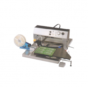
 SMT semi-automatic pick and place machine with Dispenser
 -
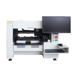
TVM925 SMT pick and place machine 4 head 38 feeders slots assembly of electronic components
-
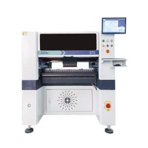
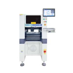
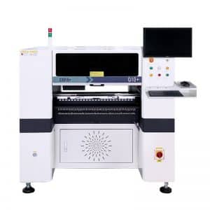
Q10 SMT Automatic pick and place machine 10 Heads 100 Slots High Precision and High Efficiency SMT/LED Assembly
-
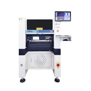
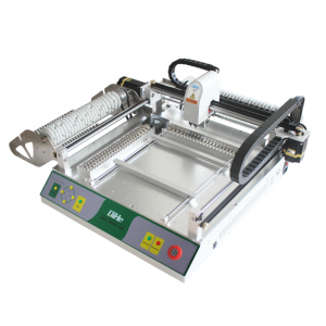
Q6 SMT pick and place machine 6heads 50slots With PCB Rail Servo Pick&Place Machine
-
Q4 SMT pick and place machine 4heads 50slots With PCB Rail Servo Pick&Place Machine
-
TVM802B Plus SMT pick and place machine 2heads 58slots desktop pick&place deluxe edition
-
QM10 SMT pick and place machine 10heads 80slots Fully Automatic Chip mounter SMT Assembly
-
TVM802BX SMT pick and place machine 2heads 46slots desktop pnp mounter deluxe edition
-
QL41 SMT pick and place machine 4heads 8slots LED for 1.2meters led strip pick&place machine
What is SMT in engineering?
Surface mount technology is a part of the electronic assembly that deals with the mounting of electronic components to the surface of a PCB. Electronic components mounted this way are called surface-mounted devices (SMD). SMT was developed to minimize manufacturing costs while making efficient use of board space.Qihe SMT company develops and produces all kinds of SMT equipment suitable for world wide market, including pnp machine,reflow oven,stencil printer,pcb handling machines,and other products.
Small desktop pick and place machine TVM802A,TVM802B,TVM802AX,TVM802BX series suitable for beginners, for hobbiest or low vol usag.
Advanced level 4-head LED strip placement QL41 led machines and with rail universal series TVM925S,TVM926S,
Fully automatic 6-10-head placement QM61,QM62,QM81,QM10,machines, which are suitable for high volume mass production in factories.
Know more about us https://www.qhsmt.com/about-qihe-smt-equipment/
Follow us on social media https://www.facebook.com/Qihesmt/
What is SMT in programming?
Offline Automated Programming vs Inline SMT Programming
Qihe pick and place machine can be programmed directly on the SMT equipment .
Or Coordinates can also be imported csv file through programming software.
Currently supported software such as protel,DXP,Altium Designer,Pads,Candes,proteus,DXP.
Inline SMT programming is a solution to consider for narrow segments of device programming requiring short programming times, with medium to high volume, for just one device type.
WHAT IS SMT pick and place machine?
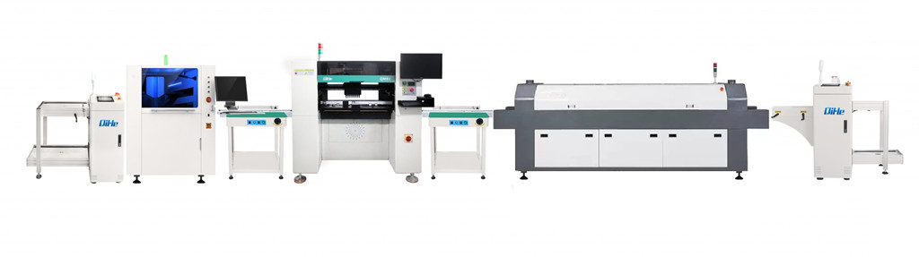
SMT (Surface Mounted Technology) is a comprehensive system engineering technology, which covers substrates, design, equipment, components, assembly processes, production accessories and management. When it comes to SMT pick and place machines, the automatic SMT production line requires automatic loading and unloading machine, automatic solder paste printing machine, placement machine, reflow soldering machine, AOI inspection equipment, conveyor,connecting table, etc. For these SMT assembly line equipment, Qihe SMT can offer you machines in prototype SMT line, small SMT production line, mass production SMT line at low SMT line cost. Contact us now if you are interested.
WHAT IS SMT ASSEMBLY LINE?
With the development of technology, future electronic products will be lighter, smaller and thinner. Traditional assembly technology can no longer meet the requirements of high-precision and high-density assembly. A new type of PCB assembly technology-SMT (Surface Mount Technology) has emerged. SMT Assembly is the use of automated machines to assemble electronic components on the surface of the circuit board. Its density, high speed, standardization and other characteristics occupies an absolute advantage in the field of circuit assembly technology. In addition, SMT assembly has a wide range of uses.
https://www.qhsmt.com/fully-automatic-smt-pick-and-place-machine-line/