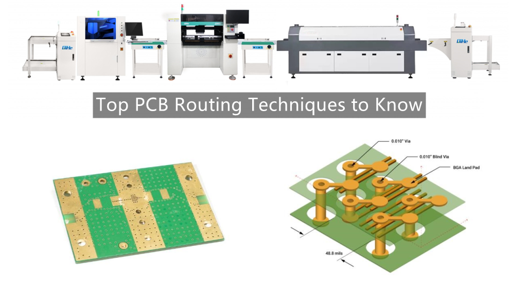
In the forum, I saw a lot of PCB wiring problems raised by netizens. I felt the problems caused by the stepping motor wiring before. I understand this PCB wiring with common sense, which is easy to understand, avoids circuit loops, electromagnetic field transmission lines, etc. Complicated things that become more and more difficult to explain, fundamentally let everyone understand what is going on, and are not bound by some professional terms, and have won the approval of most netizens. Today qihe smt pick and place machine sharing some PCB Routing Techniques to Know .
PCB wiring is the laying of roads for energized signals to connect various devices. This is like building roads and connecting cities to cars. It is exactly the same thing.
Road construction requires two lines to go and one to go back. The same is true for PCB wiring. A two-line loop needs to be formed. For low-frequency circuits, it is a loop. For high-speed electromagnetic fields, it is a transmission line. The most common such as differential signals Wire. Such as USB, network cable, etc. For the impedance characteristics of the transmission line, etc., this article will not give further explanation.
It can be said that the differential signal line is an ideal model for connecting device signals. The higher the signal requirements, the closer to the differential signal line.
Double-sided PCB boards use the bottom layer as a common reference loop
When there are many components on a board, if they are all laid out according to differential lines, one is that the PCB area is too large, and the other is that 2N lines need to be laid out. The most typical concept is the double-sided PCB board. The bottom layer is used as a common reference loop, so that only N+1 wiring is required, and the PCB layout is greatly reduced.
The public reference loop, also known as the reference ground, for most embedded industries, the signal quality requirements are not very high after digitalization, so the use of the entire layer of reference ground can reduce the size of the board and improve efficiency , which greatly saves time and is deeply loved by everyone. In fact, reducing the board area means shortening the length of the signal line, which can also partially offset the signal quality degradation caused by the reference ground. Therefore, in practice, the PCB layout effect of introducing the reference ground is basically close to the ideal model of the differential line. Today, we are all accustomed to this method. It seems that PCB wiring requires a layer of reference ground. There is no reason.
In the double-panel design, because there are often crossed wires, it is necessary to jumper the wire to the ground for cross wire exchange. This needs to be pointed out that the jumper should not be too long. If it is too long, it is easy to split the reference ground, especially for some For lines with high signal quality requirements, the reference ground at the bottom cannot be divided. Otherwise, the circuit of the signal is completely destroyed, and the reference ground loses its meaning. So generally speaking, the reference ground layer is only suitable for short jumpers of signal lines, and the signal lines should be placed on the top layer as much as possible, or more layers of PCB boards should be introduced.
If the road is too close to the road, it will easily be affected. For example, when you take the high-speed rail, you can feel the impact of the train coming from the opposite side on the train you are taking. The same is true for the signal lines, not too close. If the signal lines are parallel to each other, a certain distance must be kept. This is subject to the experiment, and there must be a good reference ground at the bottom. Under low-frequency small signals, the general impact is not very great, and high-frequency strong signals need attention.
For PCB wiring with high frequency and high current, such as switching power supply, the most taboo is that the driving signal is interfered by the output of strong current and strong voltage. The drive signal of the MOS tube is easily affected by the strong output current, so keep a certain distance between them and don’t get too close. In the era of analog audio, if the magnification of the op amp is too high, the self-excitation effect will appear, the reason is the same as that of the MOS tube.
The carrier of PCB wiring is the PCB board. Generally, the reference ground is about 1mm away from the edge of the PCB board, and the signal line is about 1mm away from the edge of the reference ground. In this way, all signals are confined within the PCB board, which can reduce EMC radiation.
When you have no concept of PCB design, just think about our daily roads, the two are exactly the same.
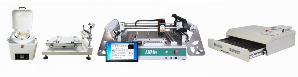
Best seller SMT Machine :Qihe smt line products
-
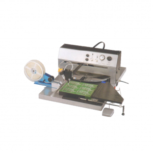
 SMT semi-automatic pick and place machine with Dispenser
 -
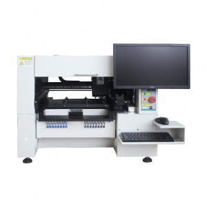
TVM925 SMT pick and place machine 4 head 38 feeders slots assembly of electronic components
-
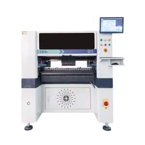
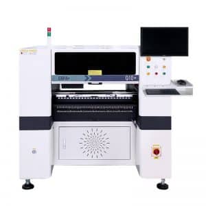
Q10 SMT Automatic pick and place machine 10 Heads 100 Slots High Precision and High Efficiency SMT/LED Assembly
-
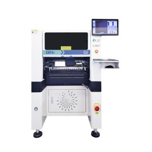
Q6 SMT pick and place machine 6heads 50slots With PCB Rail Servo Pick&Place Machine
-
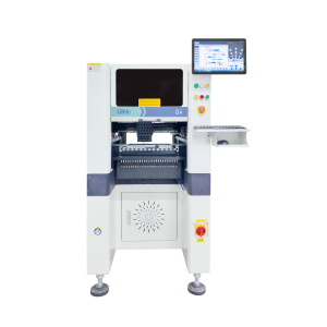
Q4 SMT pick and place machine 4heads 50slots With PCB Rail Servo Pick&Place Machine
-
TVM802B Plus SMT pick and place machine 2heads 58slots desktop pick&place deluxe edition
-
QM10 SMT pick and place machine 10heads 80slots Fully Automatic Chip mounter SMT Assembly
-
TVM802BX SMT pick and place machine 2heads 46slots desktop pnp mounter deluxe edition
-
QL41 SMT pick and place machine 4heads 8slots LED for 1.2meters led strip pick&place machine
What is SMT in engineering?
Surface mount technology is a part of the electronic assembly that deals with the mounting of electronic components to the surface of a PCB. Electronic components mounted this way are called surface-mounted devices (SMD). SMT was developed to minimize manufacturing costs while making efficient use of board space.Qihe SMT company develops and produces all kinds of SMT equipment suitable for world wide market, including pnp machine,reflow oven,stencil printer,pcb handling machines,and other products.
Small desktop pick and place machine TVM802A,TVM802B,TVM802AX,TVM802BX series suitable for beginners, for hobbiest or low vol usag.
Advanced level 4-head LED strip placement QL41 led machines and with rail universal series TVM925S,TVM926S,
Fully automatic 6-10-head placement QM61,QM62,QM81,QM10,machines, which are suitable for high volume mass production in factories.
Know more about us https://www.qhsmt.com/about-qihe-smt-equipment/
Follow us on social media https://www.facebook.com/Qihesmt/
What is SMT in programming?
Offline Automated Programming vs Inline SMT Programming
Qihe pick and place machine can be programmed directly on the SMT equipment .
Or Coordinates can also be imported csv file through programming software.
Currently supported software such as protel,DXP,Altium Designer,Pads,Candes,proteus,DXP.
Inline SMT programming is a solution to consider for narrow segments of device programming requiring short programming times, with medium to high volume, for just one device type.
WHAT IS SMT pick and place machine?
SMT (Surface Mounted Technology) is a comprehensive system engineering technology, which covers substrates, design, equipment, components, assembly processes, production accessories and management. When it comes to SMT pick and place machines, the automatic SMT production line requires automatic loading and unloading machine, automatic solder paste printing machine, placement machine, reflow soldering machine, AOI inspection equipment, conveyor,connecting table, etc. For these SMT assembly line equipment, Qihe SMT can offer you machines in prototype SMT line, small SMT production line, mass production SMT line at low SMT line cost. Contact us now if you are interested.
WHAT IS SMT ASSEMBLY LINE?
With the development of technology, future electronic products will be lighter, smaller and thinner. Traditional assembly technology can no longer meet the requirements of high-precision and high-density assembly. A new type of PCB assembly technology-SMT (Surface Mount Technology) has emerged. SMT Assembly is the use of automated machines to assemble electronic components on the surface of the circuit board. Its density, high speed, standardization and other characteristics occupies an absolute advantage in the field of circuit assembly technology. In addition, SMT assembly has a wide range of uses.
https://www.qhsmt.com/fully-automatic-smt-pick-and-place-machine-line/