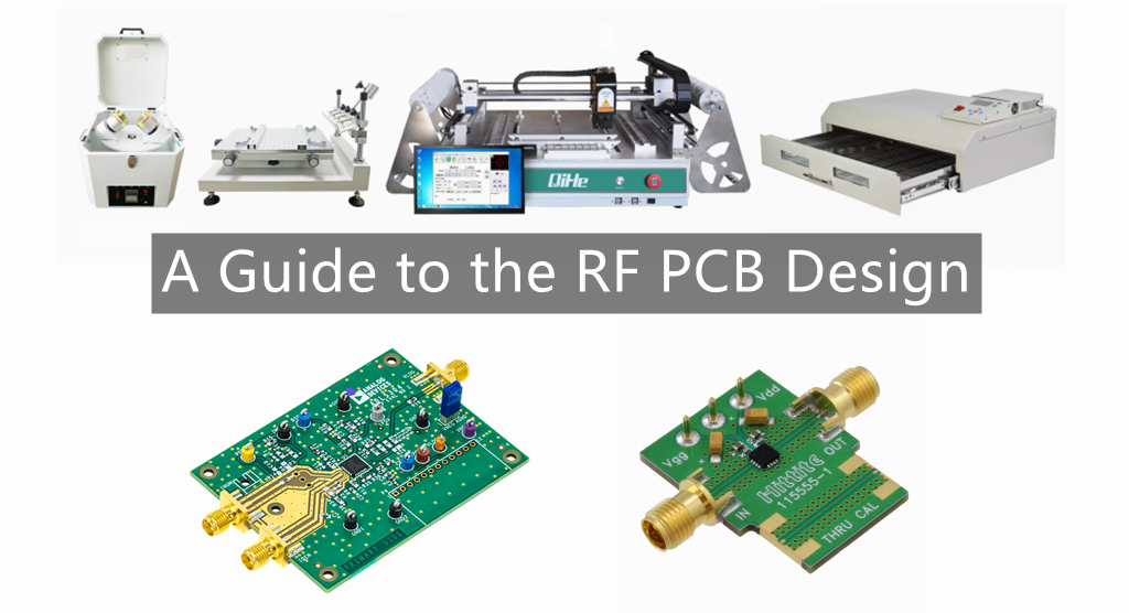
Radio frequency (RF) designs operate at high frequencies, and they require careful layout and routing to prevent signal integrity problems. An RF PCB layout can sometimes contain a section with digital components, and careful layout can help prevent interference between RF and digital signals.Today qihe smt pick and place machine sharing Some knowledge of radio frequency (RF) PCB design .
Radio frequency (RF) PCB design has many uncertainties in the current published theory, and is often described as a “black art”. Usually, for circuits in the frequency band below microwave (including low-frequency and low-frequency digital circuits), careful planning under the premise of fully grasping various design principles is the guarantee for a successful design at one time. For PC-type digital circuits with frequency bands above microwave and high frequency. You need 2~3 versions of PCB to ensure the circuit quality. For RF circuits in the frequency band above microwave, more versions are often needed: PCB design and continuous improvement, and on the premise of considerable experience. This shows that RF electrical design is difficult.
The rapid development of radio frequency integrated circuits provides broad prospects for engineers and technicians engaged in various wireless communications. But at the same time, the design of RF circuits requires designers to have certain practical experience and engineering design capabilities. Some experiences summarized in this paper can help developers of radio frequency integrated circuits shorten the development cycle. Avoid unnecessary detours and save manpower and material resources.
Common problems in RF circuit design
Interference between digital circuit modules and analog circuit modules
If the analog circuit (RF) and the digital circuit work separately, each may work fine. However, once you put the two on the same board and work together from the same power supply, the whole system is likely to be unstable. This is primarily because digital signals frequently swing between ground and the positive supply (>3 V), and with extremely short periods, often on the order of nanoseconds. Due to the larger amplitude and shorter switching times. These digital signals contain a large number of high-frequency components independent of the switching frequency. In the analog part, the signal transmitted from the wireless tuning loop to the receiving part of the wireless device is generally less than 1 μV. Therefore, the difference between the digital signal and the RF signal can reach 120 dB. Obviously. If the digital signal cannot be well separated from the radio frequency signal. Weak radio frequency signals can be corrupted, and as a result, the wireless device’s performance will deteriorate, or even not work at all.
Noise interference from power supply
RF circuits are quite sensitive to power supply noise, especially to glitch voltage and other high-frequency harmonics. Microcontrollers will suddenly draw most of the current for a short period of time during each internal clock cycle, because modern microcontrollers are manufactured in a CMOS process. therefore. Suppose a microcontroller runs at an internal clock frequency of 1MHz, at which frequency it will draw current from the power supply. If proper power supply decoupling is not taken. It will inevitably cause a voltage glitch on the power line. If these voltage spikes reach the power pins of the RF part of the circuit, it may cause work failure in severe cases.
Unreasonable ground wire
If the ground wire of the RF circuit is not handled properly, some strange phenomena may occur. For digital circuit designs, most digital circuits function well even without a ground plane. And at RF frequencies, even a very short ground lead acts like an inductor. Roughly calculated, the inductance per millimeter of length is about lnH, and the inductance of a 10 toni PCB line at 433 MHz is about 27Ω. Without a ground plane, most ground traces would be long and the circuit would not behave as designed.
Radiation interference from antenna to other analog circuit parts
In PCB circuit design, there are usually other analog circuits on the board. For example, many circuits have an analog-to-digital conversion (ADC) or a digital-to-analog converter (DAC). High-frequency signals from the antenna of the RF transmitter may reach the analog input of the ADC. Because any circuit line may send or receive RF signals like an antenna. If the processing at the ADC input is not done properly, the RF signal may self-excite within the ESD diodes at the ADC input. Thus causing ADC deviation.
RF circuit design principles and schemes
RF layout concept
When designing RF layout, the following general principles must be met first:
the
(1) Isolate the high-power RF amplifier (HPA) and the low-noise amplifier (LNA) as much as possible. Simply put, it is to keep the high-power RF transmitting circuit away from the low-power RF receiving circuit:
(2) Make sure that there is at least a whole piece of land in the high-power area on the PCB, preferably without vias on it. Of course, the larger the copper foil area, the better;
(3) Circuit and power supply decoupling is also extremely important;
(4) The RF output usually needs to be far away from the RF input;
(5) Sensitive analog signals should be kept away from high-speed digital signals and RF signals as much as possible.
Design principles of physical partition and electrical partition
The design partition can be decomposed into physical partition and electrical partition. Physical partitioning mainly involves component layout, orientation, and shielding; electrical partitioning can be further decomposed into partitions for power distribution, RF routing, sensitive circuits and signals, and grounding.
Principles of Physical Partitioning
Layout principle of component location. Component placement is the key to achieving a good RF design. The most effective technique is to first fix and orient components on the RF path so that the length of the RF path is minimized, keeping the input away from the output. And separate the high-power circuits from the low-power circuits as far as possible.
PCB stack design principles. The most efficient board stacking method is to arrange the main ground plane (main ground) on the second layer below the surface layer, and arrange the RF lines on the surface layer as much as possible. Minimizing via size on the RF path not only reduces path inductance, but also reduces virtual solder joints on the main ground and reduces the chance of RF energy leaking to other areas within the stackup.
Principles of RF devices and their RF wiring layout. In physical space, linear circuits like multistage amplifiers are usually sufficient to isolate multiple RF regions from each other, but duplexers, mixers, and IF amplifiers/mixers always have multiple RF/IF The signals interfere with each other. Care must therefore be taken to minimize this effect. RF and IF traces should be crossed as much as possible with a ground space between them as much as possible. Proper RF routing is very important to overall PCB performance, which is why component layout typically takes up the majority of time in cellular phone PCB design.
Design principles for reducing interference coupling of high/low power devices. On a cellular phone PCB, it is usually possible to place the low noise amplifier circuit on one side of the PCB and the high power amplifier on the other side, and finally connect them to the RF end and the baseband processor on the same side through a duplexer on the antenna at the end. Tricks are used to ensure that the vias do not transfer RF energy from one side of the board to the other, a common technique is to use blind vias on both sides. The adverse effects of vias can be minimized by arranging the vias in areas that are free from RF interference on both sides of the PCB.
Electrical Zoning Principles
Principle of power transmission. Most circuits in a cell phone draw relatively little DC current, so trace width is usually not an issue. but. A separate high-current line as wide as possible must be set for the power supply of the high-power amplifier to minimize the transmission voltage drop. To avoid too much current loss, multiple vias are required to pass current from one layer to another.
Power supply decoupling of high-power devices. If the high power amplifier is not adequately decoupled at its supply pins, the high power noise will radiate across the board and cause various problems. Grounding of high power amplifiers is critical and often requires the design of a metal shield.
RF input and output isolation principle. In most cases, it is also critical to keep the RF output away from the RF input. This also applies to amplifiers, buffers and filters. In the worst case, amplifiers and buffers have the potential to self-oscillate if their outputs are fed back to their inputs with proper phase and amplitude. In the best case, they will work stably at any temperature and voltage. Actually. They can become unstable and add noise and intermodulation signals onto the RF signal.
Filter input and output isolation principle. If the RF signal line has to be routed from the input to the output of the filter, this can seriously damage the bandpass characteristics of the filter. In order to make the input and output well isolated. First a circle of ground must be placed around the filter. Secondly, a ground should also be arranged in the lower layer of the filter and connected to the main ground surrounding the filter. It is also a good idea to keep the signal lines that need to pass through the filter as far away from the filter pins as possible. In addition, grounding at various points throughout the board needs to be done very carefully, or you may unknowingly introduce an undesired coupling path.
Digital circuits and analog circuits are isolated. In all PCB designs, it is a general principle to keep digital circuits as far away from analog circuits as possible, and it also applies to RF PCB design. The common analog ground and the ground used to shield and separate signal lines are usually equally important, and design changes caused by inadvertence may cause the design that is about to be completed to have to be reinvented. Also keep RF lines away from analog lines and some critical digital signals. All RF traces, pads and components should be filled with ground copper as much as possible. And as far as possible connected to the main land. If the RF trace must pass through the signal line, try to arrange a layer of ground connected to the main ground along the RF trace between them. If not possible, make sure they are criss-crossed. This minimizes capacitive coupling while spreading as much ground as possible around each RF trace and connecting them to the main ground. also. Minimizing the distance between parallel RF traces minimizes inductive coupling.
Read more: A Guide to the RF PCB DesignBest seller SMT Machine :Qihe smt line products
-
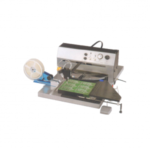
 SMT semi-automatic pick and place machine with Dispenser
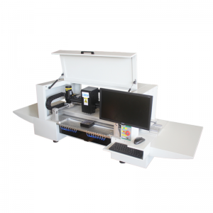
 -
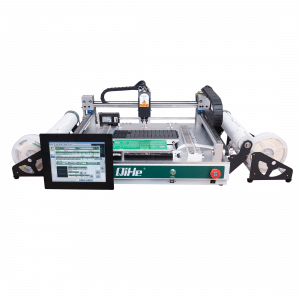
TVM925 SMT pick and place machine 4 head 38 feeders slots assembly of electronic components
-
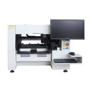
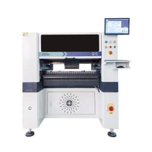
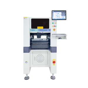
Q10 SMT Automatic pick and place machine 10 Heads 100 Slots High Precision and High Efficiency SMT/LED Assembly
-
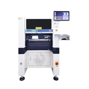
Q6 SMT pick and place machine 6heads 50slots With PCB Rail Servo Pick&Place Machine
-
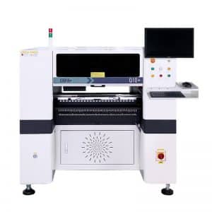
Q4 SMT pick and place machine 4heads 50slots With PCB Rail Servo Pick&Place Machine
-
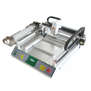
TVM802B Plus SMT pick and place machine 2heads 58slots desktop pick&place deluxe edition
-
QM10 SMT pick and place machine 10heads 80slots Fully Automatic Chip mounter SMT Assembly
-
TVM802BX SMT pick and place machine 2heads 46slots desktop pnp mounter deluxe edition
-
QL41 SMT pick and place machine 4heads 8slots LED for 1.2meters led strip pick&place machine
What is SMT in engineering?
Surface mount technology is a part of the electronic assembly that deals with the mounting of electronic components to the surface of a PCB. Electronic components mounted this way are called surface-mounted devices (SMD). SMT was developed to minimize manufacturing costs while making efficient use of board space.Qihe SMT company develops and produces all kinds of SMT equipment suitable for world wide market, including pnp machine,reflow oven,stencil printer,pcb handling machines,and other products.
Small desktop pick and place machine TVM802A,TVM802B,TVM802AX,TVM802BX series suitable for beginners, for hobbiest or low vol usag.
Advanced level 4-head LED strip placement QL41 led machines and with rail universal series TVM925S,TVM926S,
Fully automatic 6-10-head placement QM61,QM62,QM81,QM10,machines, which are suitable for high volume mass production in factories.
Know more about us https://www.qhsmt.com/about-qihe-smt-equipment/
Follow us on social media https://www.facebook.com/Qihesmt/
What is SMT in programming?
Offline Automated Programming vs Inline SMT Programming
Qihe pick and place machine can be programmed directly on the SMT equipment .
Or Coordinates can also be imported csv file through programming software.
Currently supported software such as protel,DXP,Altium Designer,Pads,Candes,proteus,DXP.
Inline SMT programming is a solution to consider for narrow segments of device programming requiring short programming times, with medium to high volume, for just one device type.
WHAT IS SMT pick and place machine?
SMT (Surface Mounted Technology) is a comprehensive system engineering technology, which covers substrates, design, equipment, components, assembly processes, production accessories and management. When it comes to SMT pick and place machines, the automatic SMT production line requires automatic loading and unloading machine, automatic solder paste printing machine, placement machine, reflow soldering machine, AOI inspection equipment, conveyor,connecting table, etc. For these SMT assembly line equipment, Qihe SMT can offer you machines in prototype SMT line, small SMT production line, mass production SMT line at low SMT line cost. Contact us now if you are interested.
WHAT IS SMT ASSEMBLY LINE?
With the development of technology, future electronic products will be lighter, smaller and thinner. Traditional assembly technology can no longer meet the requirements of high-precision and high-density assembly. A new type of PCB assembly technology-SMT (Surface Mount Technology) has emerged. SMT Assembly is the use of automated machines to assemble electronic components on the surface of the circuit board. Its density, high speed, standardization and other characteristics occupies an absolute advantage in the field of circuit assembly technology. In addition, SMT assembly has a wide range of uses.
https://www.qhsmt.com/fully-automatic-smt-pick-and-place-machine-line/