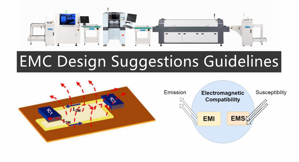
The basic causes of EMC problems are fairly common and mostly have to do with design flaws that cause interference among the traces, circuits, vias, PCB coils and other elements. These essential design principles can help prevent and fix these electromagnetic problems in a printed circuit board design.Today qihe smt pick and place machine sharing Ten tips for EMC Design Suggestions Guidelines.
Design of the ground plane.
A low inductance ground loop is the most effective way to suppress EMC problems during PCB design. Expanding the ground plane area and reducing the inductive reactance of the ground loop can effectively reduce radiation and crosstalk.
There are many ways to design the signal ground loop. The worse method is to randomly connect the device to the ground network. This high inductance ground loop design can cause unexpected EMC problems.
The recommended approach is to use a complete ground plane to provide the lowest impedance path for signals to return. Obviously, with a two-layer PCB, a full ground plane is impractical. In this case, the designer can use the ground grid method, as shown in Figure 1a. In this case, the loop inductance depends on the grid spacing.
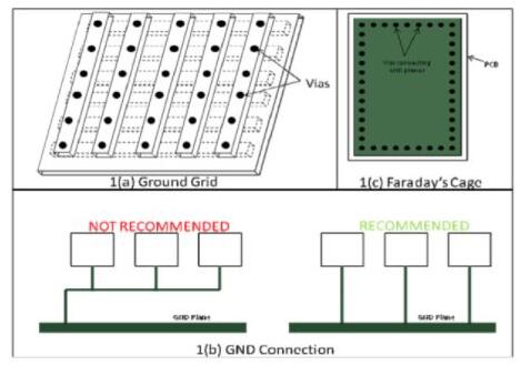
Signal return is very important. A longer return path means a larger return path, resulting in an antenna effect and radiated energy. Therefore, the signal return should take the shortest path and be directly connected to the ground plane. It is not advisable to connect all points at a single point and then connect them together to the ground plane, which not only increases the current loop size, but also increases the possibility of ground bounce. Figure 1b illustrates the recommended connection of the device to the ground plane.
Faraday cages are another way to reduce EMC problems. The Faraday cage is a circle of stitching holes added around the periphery of the PCB. Pay attention to the fact that there are no traces outside the cage.
As shown in Figure 1c, the Faraday cage effectively suppresses the radiation/interference from the PCB to/from outside the board. It is recommended to connect all GND holes with a ground wire with a width of 200~400mils on the surface layer; on the signal layer, it is recommended to connect these GND holes with a ground wire with a width of 20~40mils, but it is not recommended to connect the wires to form a loop.
Device isolation
According to the function, the components are grouped, and different groups are placed in different positions on the PCB board, such as analog signals, digital signals, power supply parts, low-speed signals and high-speed signals, etc. The signals of each group should be in their respective assigned areas, and the signals passing between different groups (from one subsystem to another) should add filtering measures at the boundary.
Stacked design
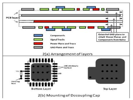
Designs with more than two layers of boards should have a complete ground plane. In a four-layer board… it should be noted that there should be a GND layer between the high-speed signal layer and the high-speed signal line. For two-layer boards, a complete GND plane is not practical, and a ground grid method can be used. If there is no separate power plane, it is recommended to run the GND line in parallel under the power trace to ensure the stability of the power supply.
Digital circuits
When dealing with digital circuits, pay special attention to clock signals and high-speed signal lines. These signal traces should be as short as possible and close to the ground plane to ensure that radiation and crosstalk are within a controllable range. For these signals, be careful to reduce the use of vias and avoid routing traces on the edge of the PCB or close to the connector. These signals should also be kept away from the power plane, as they may couple noise into the power plane.
For the handling of the oscillator, in addition to isolating it with GND. Be careful not to run the signal line parallel or under the oscillator, and ensure there is sufficient distance from the CLK signal. Keep the oscillator as close as possible to the chip that uses the clock.
Note that return flow always follows the path of lowest impedance. Therefore, the GND of the load return flow should be as close as possible to its signal path to minimize the current loop area.
The P/N lines between the differential pairs are close to each other, which can effectively perform common mode suppression.
Clock termination
Pay attention to the impedance matching of the clock signal line, otherwise it will cause signal reflection. If the reflected signals are not processed, they will be radiated. There are many valid termination methods, including source termination, end termination, and AC termination.
Analog circuits
Analog signals should be kept away from high-speed transition signals and isolated by GND. Low-pass filters are commonly used in applications to filter out high-frequency noise from surrounding analog signals. In addition, the analog and digital grounds should be separated.
Decoupling capacitor
Any noise on the power supply may cause the device to work abnormally. Generally speaking, what is coupled to the power supply is some high-frequency noise, which can be filtered out by using a decoupling capacitor. The decoupling capacitor provides power for high-frequency noise. Low impedance path to GND. The signal return path forms a loop structure from the power supply to the ground, and the decoupling capacitor is placed as close as possible to the IC pins to minimize the area of the return loop. A large area return loop increases radiation and becomes a potential cause of EMC failure.
Theoretically, the reactance value of the capacitor gradually approaches zero as the frequency increases. However, such an ideal situation does not exist, and the package and pins will increase the equivalent inductance value of the capacitor. Using multiple low-ESL capacitors at the same time helps to enhance the decoupling effect.
Cables
Many EMC problems are caused by cables acting as antennas when high-speed signals pass through them. Ideally, current flows into the cable at one end and flows out without attenuation at the other end. The actual situation is that the existence of parasitic capacitance and inductance will cause radiation, resulting in EMI problems. Coupling can be kept low by suppressing the induced magnetic field through the twisted pair. When using stripline, take care to provide multiple GND returns (multiple GND lines). For high-frequency signals, GND shielding wires should be provided at both ends of the cable.
Crosstalk
Crosstalk exists between any two traces on the PCB, and the size of the crosstalk is related to mutual inductance, mutual capacitance, edge rate of the signal, and impedance of the trace. In digital systems, the crosstalk caused by mutual inductance is generally greater than the crosstalk caused by mutual capacitance. The mutual inductance between the signal lines can be reduced by increasing the distance between the signal lines, or reducing the distance between the signal lines and GND.
Shielding
Shielding is not an electronic method of reducing EMC, but a mechanical means. Metallic (conductive or magnetic material) enclosures can be used to shield EMI from outside the system. According to actual requirements, shielding can be for part or for the whole. The shielding cavity is equivalent to a closed grounded container, which can effectively absorb and reflect radiation to reduce the size of the loop antenna. Likewise, shielding can also be the separation between different parts, attenuating the energy radiated from one part to another. Shielding achieves the effect of reducing EMI by attenuating the E parameter and H parameter of the radiated wave!
Read more: Ten tips for EMC Design Suggestions GuidelinesBest seller SMT Machine :Qihe smt line products
-
 SMT semi-automatic pick and place machine with Dispenser
 -
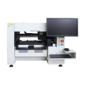
TVM925 SMT pick and place machine 4 head 38 feeders slots assembly of electronic components
-
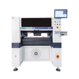
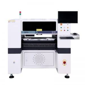
Q10 SMT Automatic pick and place machine 10 Heads 100 Slots High Precision and High Efficiency SMT/LED Assembly
-
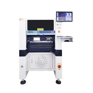
Q6 SMT pick and place machine 6heads 50slots With PCB Rail Servo Pick&Place Machine
-
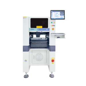
Q4 SMT pick and place machine 4heads 50slots With PCB Rail Servo Pick&Place Machine
-
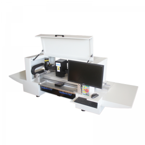
TVM802B Plus SMT pick and place machine 2heads 58slots desktop pick&place deluxe edition
-
QM10 SMT pick and place machine 10heads 80slots Fully Automatic Chip mounter SMT Assembly
-
TVM802BX SMT pick and place machine 2heads 46slots desktop pnp mounter deluxe edition
-
QL41 SMT pick and place machine 4heads 8slots LED for 1.2meters led strip pick&place machine
What is SMT in engineering?
Surface mount technology is a part of the electronic assembly that deals with the mounting of electronic components to the surface of a PCB. Electronic components mounted this way are called surface-mounted devices (SMD). SMT was developed to minimize manufacturing costs while making efficient use of board space.Qihe SMT company develops and produces all kinds of SMT equipment suitable for world wide market, including pnp machine,reflow oven,stencil printer,pcb handling machines,and other products.pick and place
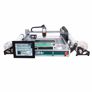
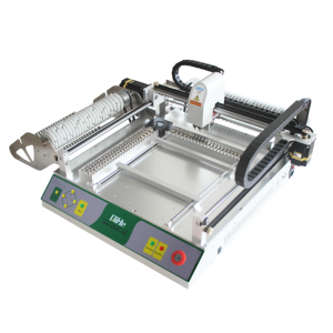
Small desktop pick and place machine TVM802A,TVM802B,TVM802AX,TVM802BX series suitable for beginners, for hobbiest or low vol usag.
Advanced level 4-head LED strip placement QL41 led machines and with rail universal series TVM925S,TVM926S,pick and place
Fully automatic 6-10-head placement QM61,QM62,QM81,QM10,machines, which are suitable for high volume mass production in factories.
Know more about us https://www.qhsmt.com/about-qihe-smt-equipment/
Follow us on social media https://www.facebook.com/Qihesmt/
What is SMT in programming?
Offline Automated Programming vs Inline SMT Programming
Qihe pick and place machine can be programmed directly on the SMT equipment .
Or Coordinates can also be imported csv file through programming software.
Currently supported software such as protel,DXP,Altium Designer,Pads,Candes,proteus,DXP.
Inline SMT programming is a solution to consider for narrow segments of device programming requiring short programming times, with medium to high volume, for just one device type.
WHAT IS SMT pick and place machine?
SMT (Surface Mounted Technology) is a comprehensive system engineering technology, which covers substrates, design, equipment, components, assembly processes, production accessories and management. When it comes to SMT pick and place machines, the automatic SMT production line requires automatic loading and unloading machine, automatic solder paste printing machine, placement machine, reflow soldering machine, AOI inspection equipment, conveyor,connecting table, etc. For these SMT assembly line equipment, Qihe SMT can offer you machines in prototype SMT line, small SMT production line, mass production SMT line at low SMT line cost. Contact us now if you are interested.pick and place
WHAT IS SMT ASSEMBLY LINE?
With the development of technology, future electronic products will be lighter, smaller and thinner. Traditional assembly technology can no longer meet the requirements of high-precision and high-density assembly. A new type of PCB assembly technology-SMT (Surface Mount Technology) has emerged. SMT Assembly is the use of automated machines to assemble electronic components on the surface of the circuit board. Its density, high speed, standardization and other characteristics occupies an absolute advantage in the field of circuit assembly technology. In addition, SMT assembly has a wide range of uses.
https://www.qhsmt.com/fully-automatic-smt-pick-and-place-machine-line/