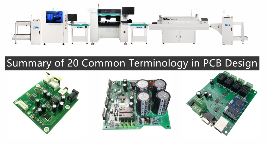
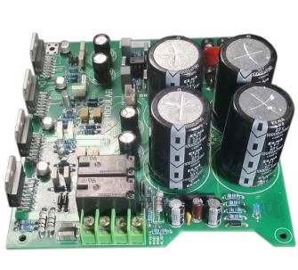
PCB (Printed Circuit Board): A printed circuit board is a printed board composed of conductive materials and insulating substrates, which realizes the signal connection of the designed circuit and assembles all the components required for the circuit.Today qihe smt pick and place machine sharing summary of 20 commonly used terms in PCB design PCB .
Single layer PCB: A PCB with only one side for signal wiring. Double sided PCB: A PCB with signal wiring on both sides.
Multilayer PCB: There are many conductive wiring layers and insulation material layers bonded together, and signal wiring between layers can achieve interconnection of PCBs.
Printed Circuit: A printed component or printed circuit generated by design on an insulating substrate, as well as a signal transmission circuit combining the two.
Layer: A conductive layer composed of copper foil on a PCB, including a transmission signal layer and a power or ground layer.
Inner Layer: The inner layer is a negative layer of a PCB, mainly used as a layer for power or ground.
Signal Layer: The signal layer is a type of positive layer on a PCB, mainly used for signal transmission and routing.
Single layer PCB: A PCB with only one side for signal wiring.
Mother Board: A main PCB that can install one or more PCB components.
Backplane: Multiple connector sockets are provided on one side for electrical interconnection of PCBs between points. Electrical interconnections between points can be printed circuits.
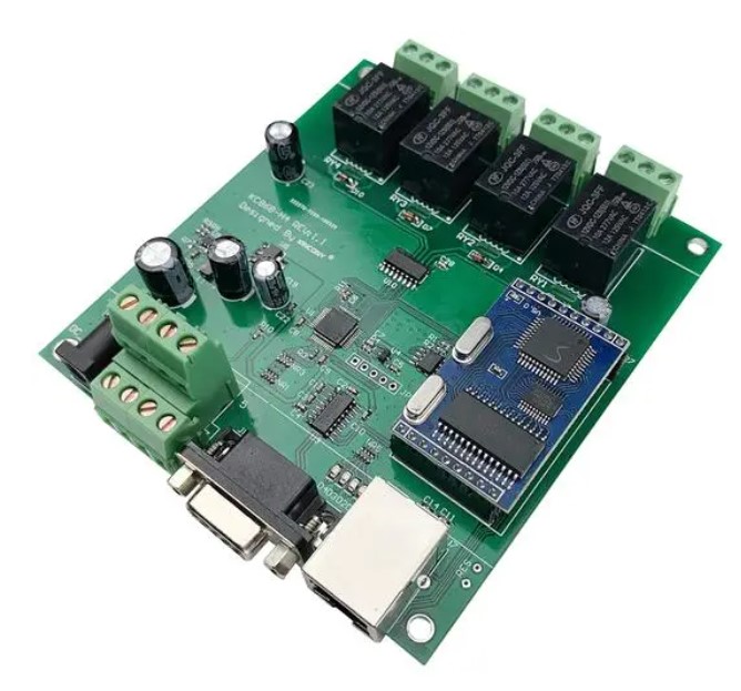
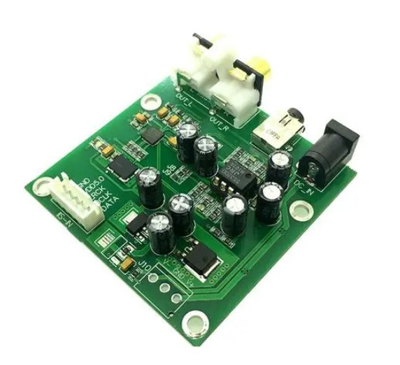
Components: Basic units that implement circuit functions, such as capacitors, inductors, resistors, integrated circuit chips, etc.
Footprint: Component packaging refers to the appearance and pad position of a component when soldered onto a circuit board. Since the packaging of the original component is only about the appearance and pad position of the component, pure component packaging is only a concept of space. Therefore, different components can share the same component packaging.
Pad: An electrical soldering point used to connect component pins and PCB wiring, typically consisting of a copper layer, copper plating, and solder flow, with a solder mask layer around it.
Via: To connect the lines between layers, a common hole is drilled at the intersection of the wires that need to be connected in each layer.
Blind Via: A through hole that extends from the middle layer to a surface layer of a PCB.
Buried Via: A through hole from one middle to another that does not extend to the surface layer of a PCB.
Clearance: The minimum distance to prevent short circuits between signals, which is an important setting parameter for PCB wiring.
Layout: The operation of placing components appropriately on a PCB based on design requirements and circuit characteristics. It is an important step in implementing wiring, and a good layout can effectively achieve the routing of all signals on the PCB.
Net List: A data table representing the connection relationships between component pins on a PCB, which describes all electrical connections on the PCB.
Routing: The operation of connecting all electrical connections with actual wiring according to the network table and design requirements after the layout is completed. Usually, manual intervention in automatic wiring is used for PCB design
Read more: Summary of 20 Common Terminology in PCB DesignBest seller SMT Machine :Qihe smt line products
-
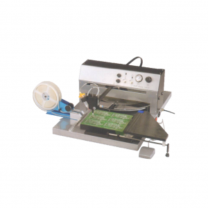
 SMT semi-automatic pick and place machine with Dispenser
 -
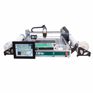
TVM925 SMT pick and place machine 4 head 38 feeders slots assembly of electronic components
-
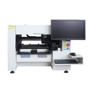
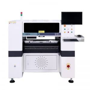
Q10 SMT Automatic pick and place machine 10 Heads 100 Slots High Precision and High Efficiency SMT/LED Assembly
-
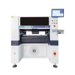
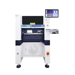
Q6 SMT pick and place machine 6heads 50slots With PCB Rail Servo Pick&Place Machine
-
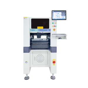
Q4 SMT pick and place machine 4heads 50slots With PCB Rail Servo Pick&Place Machine
-
TVM802B Plus SMT pick and place machine 2heads 58slots desktop pick&place deluxe edition
-
QM10 SMT pick and place machine 10heads 80slots Fully Automatic Chip mounter SMT Assembly
-
TVM802BX SMT pick and place machine 2heads 46slots desktop pnp mounter deluxe edition
-
QL41 SMT pick and place machine 4heads 8slots LED for 1.2meters led strip pick&place machine
What is SMT in engineering?
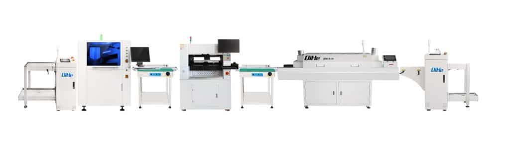
Surface mount technology is a part of the electronic assembly that deals with the mounting of electronic components to the surface of a PCB. Electronic components mounted this way are called surface-mounted devices (SMD). SMT was developed to minimize manufacturing costs while making efficient use of board space.Qihe SMT company develops and produces all kinds of SMT equipment suitable for world wide market, including pnp machine,reflow oven,stencil printer,pcb handling machines,and other products.
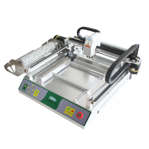
Small desktop pick and place machine TVM802A,TVM802B,TVM802AX,TVM802BX series suitable for beginners, for hobbiest or low vol usag.
Advanced level 4-head LED strip placement QL41 led machines and with rail universal series Q4,TVM925S,TVM926S,pick and place
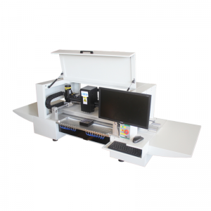
Fully automatic 6-10-head placement QM61,QM62,QM81,QM10,machines, which are suitable for high volume mass production in factories.
Know more about us https://www.qhsmt.com/about-qihe-smt-equipment/
Follow us on social media https://www.facebook.com/Qihesmt/
What is SMT in programming?
Offline Automated Programming vs Inline SMT Programming
Qihe pick and place machine can be programmed directly on the SMT equipment .
Or Coordinates can also be imported csv file through programming software.
Currently supported software such as protel,DXP,Altium Designer,Pads,Candes,proteus,DXP.
Inline SMT programming is a solution to consider for narrow segments of device programming requiring short programming times, with medium to high volume, for just one device type.