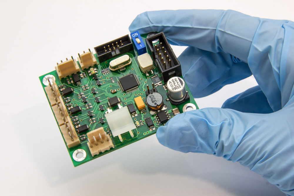
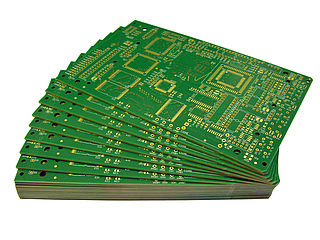
Copper plays a conductive role in printed circuit boards (PCBs). As a reactive chemical, copper is prone to oxidation when exposed to atmospheric humidity, thereafter leading to problems that may occur in high-temperature soldering, which is detrimental to the reliability of the components mounted on the PCB and the final product. Surface treatments serve two key functions: to protect the copper from oxidation and to provide a soldering surface when components are assembled on the PCB.Today qihe smt pick and place machine sharing General Knowledge of PCB OSP Surface Finish .
Circuit board surface treatments can be divided into different classifications based on the different technologies and chemicals involved, HASL (Hot Air Solder Scaling), Immersion Tin/Silver, OSP, ENIG and ENEPIG etc. Among all surface treatments, its low cost and environmentally friendly properties add even more necessity to our better understanding of it. This is what this article aims to tell you. OSP (Organic Solderability Preservative) Introduction OSP is the abbreviation of “Organic Solderability Preservative”, also known as rust inhibitor. It refers to an organic surface created by adsorption onto clean and bare copper. On the one hand, this organic finish can.
Stops copper oxidation, thermal shock and humidity. On the other hand, during the later stages of soldering, the flux must be easily removed by the flux, so that the exposed clean copper can be connected with the molten solder, thus producing solder joints in a very short time.
The applied water-based compounds belong to the azoles, such as benzotriazoles, imidazoles and benzimidazoles, all of which are adsorbed on the copper surface and form coordination with copper atoms to produce a thin film. In terms of film thickness, films prepared by benzotriazole are thin, while films prepared by imidazole are relatively thick. Differences in thickness can have a noticeable impact on board performance, which will be discussed later in this article.
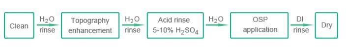
OSP manufacturing process
In fact, the history of OSP is even longer than the history of SMT (surface mount technology). This is the manufacturing process of OSP.
Note: DI refers to deionization. The “cleaning” function is to remove organic pollutants such as oil stains, fingerprints, and oxide films to keep the surface of the copper foil clean and bright. This step plays a vital role in the quality of the preservative.
Poor cleaning can result in uneven preservative thickness. In order to ensure the high quality of the finished OSP membrane, on the one hand, the concentration of the cleaning solution is controlled within the standard range through chemical laboratory analysis.
On the other hand, it is recommended to check the cleaning effect as often as possible. Once the effect is not up to standard, the cleaning fluid should be replaced in time. In the process of enhanced surface treatment, micro-etching is usually used to basically eliminate the oxidation generated on the copper foil, thereby improving the bonding force between the copper foil and the OSP solution. The speed of micro-etching directly affects the film formation rate.
Therefore, in order to obtain a smooth and uniform film thickness, it is crucial to maintain the stability of the micro-etching speed. Generally speaking, it is appropriate to control the micro-etching speed in the range of 1.0 to 1.5 microns per minute. It is best to use deionized water to rinse before the anti-corrosion agent is established to prevent the OSP solution from being contaminated by other ions, which will cause reflow soldering. Fading occurs. Likewise, it is best to use DI rinses after the preservative has been established with a pH between 4.0 and 7.0 to prevent damage to the preservative due to contamination.
Advantages of OSP
The advantages of OSP can be summarized as:
•Simple process and reusable: OSP-coated circuit boards can be easily remade by PCB manufacturers so that a new coating can be used once the PCB assembler discovers that the coating has been damaged.
•Good wetting: OSP-coated circuit boards perform better in terms of solder wetting when the flux encounters vias and pads.
•Environmentally friendly: Since water-based compounds are used in the generation process of OSP, they will not cause harm to the environment and will only fall into people’s expectations for a green world. Therefore, OSP is the best choice for electronic products that comply with green regulations such as RoHS. .
•PCB Cost Effectiveness: Due to the simple compounds applied in the OSP manufacturing process as well as the simple manufacturing process, the cost of OSP is outstanding in all types of surface treatments. It costs less, resulting in a lower final board cost.
Reflow soldering suitable for double-sided SMT assembly: With the continuous development and progress of OSP, it has been accepted by single-sided SMT assembly and double-sided SMT assembly, greatly broadening its application fields.
Lower requirements for solder mask ink: Long storage time Storage requirements for PCBs using OSP Since the preservative produced by OSP technology is very thin and easy to cut, great care must be taken during shipping and transportation. When PCBs with OSP surface treatment are exposed to high temperatures and high humidity for a long time, oxidation may occur on the PCB surface, which often results in low solderability.
Therefore, storage methods must adhere to these principles:
A vacuum package should be used with desiccant and humidity display card. Place release paper between PCBs to prevent friction from damaging the PCB surface. These PCBs cannot be exposed to direct sunlight.
Good storage environment requirements include: relative humidity (30-70% RH), temperature (15-30°C) and storage time (less than 12 months) C. During the manufacturing process, hands are not allowed to touch the OSP PCB directly to avoid oxidation due to contact with sweat. Possible problems and solutions after OSP welding Sometimes, the color of the OSP board will change after welding, which is mainly related to the thickness of the anticorrosive agent, the amount of micro-etching, the number of welding times, and abnormal contaminants. Fortunately, this problem can only be observed from the appearance.
There are usually two situations:
For environment #1, flux can help eliminate oxidation during the soldering process so that it does not affect soldering performance. Therefore, no further measurements are necessary. Instead, environment #2 happens,
Because the integrity of the OSP has been destroyed, the flux cannot eliminate the oxidation, which will greatly reduce the soldering performance.
Therefore, to ensure appearance and performance, some improvements and measurements must be made, including:
•The thickness of OSP must be controlled within a certain range.
•The number of micro-etchings must be controlled within a certain range.
•During the PCB manufacturing process, contaminants (gel residue, ink, etc.) must be 100% eliminated to prevent partial anomalies and poor solderability. Chemical mechanism of OSP thickness formation As mentioned earlier, the thickness of the film varies with the application of different ions. In the OSP solution, there are several copper ions plus three charges, and the OSP solution can dissociate in an acidic solution. After cleaning and micro-etching, the PCBs are placed into the OSP bath.
When positively charged copper ions are created around exposed copper on a PCB. Then, the empty electrons of copper ions on the copper surface are charged twice in the decomposition solution and complexed, so that 2d10 copper can be used to form a dipole bond. Finally, a complex network of preservatives is formed.
The key to OSP technology lies in the control of OSP thickness. Basically, there is a misconception that the thicker the preservative, the more protection it provides for tin soldering. In fact, if the preservative is too thick, it will be difficult for the flux to remove the preservative during welding.
A large number of studies have shown that when the OSP preservative is too thick, the spreading speed of the solder paste will be reduced, copper will be exposed at any time, the contact resistance will increase, and it will even be difficult to form solder joints. However, if the film is too thin, the thermal shock resistance will be reduced, so it will not withstand high temperatures during reflow, thus affecting the soldering performance. Therefore, generally speaking, the thickness of the preservative should be controlled within the range of 0.2~0.5μm.
When producing panels, surface roughness must be strictly controlled before leaving the workshop. For example, PCBCart’s PCB manufacturing complies with the guidelines and regulations of standard IPC 2. In addition, more than 10 years of experience and time of experimentation enable engineers to obtain the optimal solution concentration and conveyor belt moving speed to further refine the OSP thickness.
Read more: General Knowledge of PCB OSP Surface FinishBest seller SMT Machine :Qihe smt line products
-
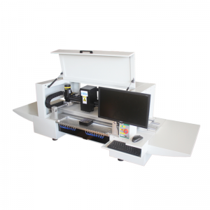
 SMT semi-automatic pick and place machine with Dispenser
 -
TVM925 SMT pick and place machine 4 head 38 feeders slots assembly of electronic components
-
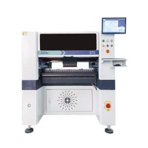
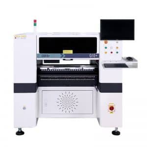
Q10 SMT Automatic pick and place machine 10 Heads 100 Slots High Precision and High Efficiency SMT/LED Assembly
-
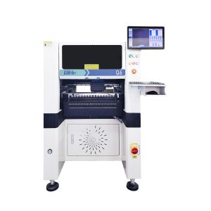
Q6 SMT pick and place machine 6heads 50slots With PCB Rail Servo Pick&Place Machine
-
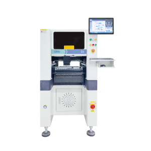
Q4 SMT pick and place machine 4heads 50slots With PCB Rail Servo Pick&Place Machine
-
TVM802B Plus SMT pick and place machine 2heads 58slots desktop pick&place deluxe edition
-
QM10 SMT pick and place machine 10heads 80slots Fully Automatic Chip mounter SMT Assembly
-
TVM802BX SMT pick and place machine 2heads 46slots desktop pnp mounter deluxe edition
-
QL41 SMT pick and place machine 4heads 8slots LED for 1.2meters led strip pick&place machine
What is SMT in engineering?
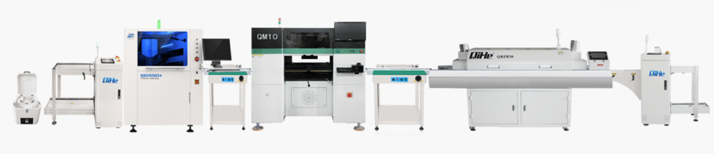
Surface mount technology is a part of the electronic assembly that deals with the mounting of electronic components to the surface of a PCB. Electronic components mounted this way are called surface-mounted devices (SMD). SMT was developed to minimize manufacturing costs while making efficient use of board space.Qihe SMT company develops and produces all kinds of SMT equipment suitable for world wide market, including pnp machine,reflow oven,stencil printer,pcb handling machines,and other products.
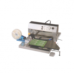
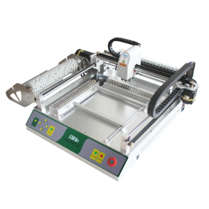
Small desktop pick and place machine TVM802A,TVM802B,TVM802AX,TVM802BX series suitable for beginners, for hobbiest or low vol usag.
Advanced level 4-head LED strip placement QL41 led machines and with rail universal series TVM925S,TVM926S,pick and place
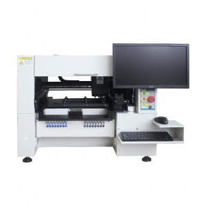
Fully automatic 6-10-head placement QM61,QM62,QM81,QM10,machines, which are suitable for high volume mass production in factories.
Know more about us https://www.qhsmt.com/about-qihe-smt-equipment/
Follow us on social media https://www.facebook.com/Qihesmt/
What is SMT in programming?
Offline Automated Programming vs Inline SMT Programming
Qihe pick and place machine can be programmed directly on the SMT equipment .
Or Coordinates can also be imported csv file through programming software.
Currently supported software such as protel,DXP,Altium Designer,Pads,Candes,proteus,DXP.
Inline SMT programming is a solution to consider for narrow segments of device programming requiring short programming times, with medium to high volume, for just one device type.
WHAT IS SMT pick and place machine?
SMT (Surface Mounted Technology) is a comprehensive system engineering technology, which covers substrates, design, equipment, components, assembly processes, production accessories and management. When it comes to SMT pick and place machines, the automatic SMT production line requires automatic loading and unloading machine, automatic solder paste printing machine, placement machine, reflow soldering machine, AOI inspection equipment, conveyor,connecting table, etc. For these SMT assembly line equipment, Qihe SMT can offer you machines in prototype SMT line, small SMT production line, mass production SMT line at low SMT line cost. Contact us now if you are interested.pick and place.pick and place machines,smt machine price,smt machine supplier,suction nozzle,smt assembly,feeder,stock in eu,pcb printer,openpnp feeder,openpnp,pcb pick and place,smt nozzle,smt line,smt meaning,smt process,smt setup,pnp machine,pcb assembly,p&p machine,p&p,pick&place,pick&place machine,pnp,stencil printer,reflow oven,pick and place machine,SMT equipment,smd machine,smt machine,SMT pick and place machine,pick and place machine,smt pick and place.
WHAT IS SMT ASSEMBLY LINE?
With the development of technology, future electronic products will be lighter, smaller and thinner. Traditional assembly technology can no longer meet the requirements of high-precision and high-density assembly. A new type of PCB assembly technology-SMT (Surface Mount Technology) has emerged. SMT Assembly is the use of automated machines to assemble electronic components on the surface of the circuit board. Its density, high speed, standardization and other characteristics occupies an absolute advantage in the field of circuit assembly technology. In addition, SMT assembly has a wide range of uses.
https://www.qhsmt.com/fully-automatic-smt-pick-and-place-machine-line/