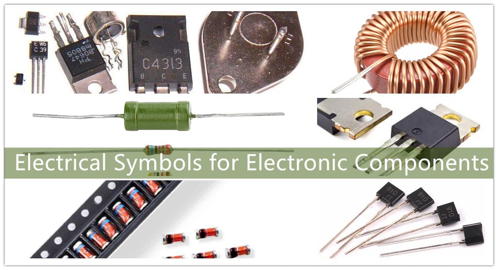
In pcb circuit diagrams, graphical symbols identify network components and devices. International letter symbolism is based on the Roman and Greek alphabets. Qihe SMT Line Equipment today will share with you some common symbols and their meanings . Electronic Components,like Resistance,Capacitance,Crystal diode,Zener diode,Inductance,Varactor diode,Transistor,Field Effect Transistor Amplifier,FET,transistor,
Resistance
Symbol representation method: Resistance is represented by “R” plus numbers in the circuit, such as: R15 represents the resistance numbered 15. The main functions of resistors in the circuit are shunting, current limiting, voltage dividing, biasing, filtering (used in combination with capacitors) and impedance matching.
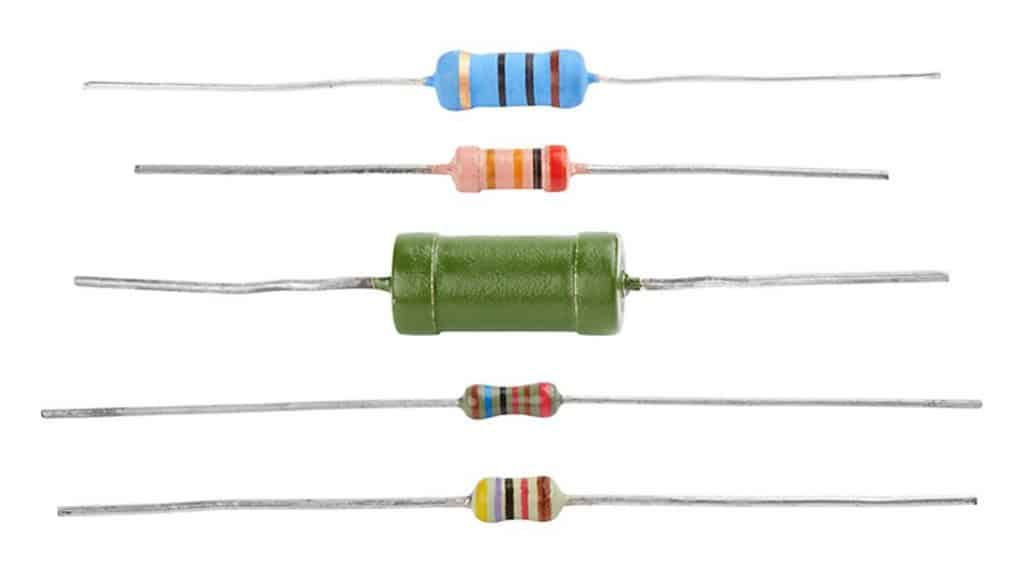
Parameter identification: the unit of resistance is ohm (Ω), and the unit of magnification is: kilohm (KΩ), megohm (MΩ), etc. The conversion method is: 1 megohm = 1000 kilohm = 1000000 ohm.
There are three methods for marking the parameters of resistors, namely, direct marking method, color marking method and digital marking method. The digital marking method is mainly used for small-volume circuits such as patches, such as: 472 means 47×102Ω (ie 4.7K); 104 means 100K The color ring marking method is most used.
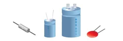
Capacitance
Representation method
Capacitance is generally represented by “C” plus numbers in the circuit (for example, C25 represents the capacitance numbered 25). A capacitor is an element composed of two metal films that are close together and separated by an insulating material. The characteristic of the capacitor is mainly to block DC and communicate with AC. The size of the capacitor capacity is the size of the electric energy that can be stored. The hindering effect of the capacitor on the AC signal is called capacitive reactance, which is related to the frequency and capacitance of the AC signal. Capacitive reactance XC=1/2πfc (f represents the frequency of the AC signal, C represents the capacitance), and the types of capacitors commonly used in telephones include electrolytic capacitors, ceramic capacitors, chip capacitors, monolithic capacitors, tantalum capacitors and polyester capacitors, etc. .
Identification method:
The identification method of capacitance is basically the same as that of resistance, which can be divided into three types: direct marking method, color marking method and digital marking method. The basic unit of capacitance is Farad (F), and other units include: Millifarad (mF), Microfarad (uF), Nanofarad (nF), and Picofarad (pF). Among them: 1 farad = 103 millifarads = 106 microfarads = 109 nanofarads = 1012 picofarads. The capacitance value of a capacitor with a large capacity is directly marked on the capacitor, such as 10uF/16V, and the capacitance value of a capacitor with a small capacity is written on the capacitor. Representation or digital representation, letter representation: 1m=1000uF, 1P2=1.2PF, 1n=1000PF, digital representation: generally use three digits to represent the capacity, the first two digits represent significant figures, and the third digit is the magnification. For example: 102 means 10×102PF=1000PF 224 means 22×104PF=0.22 uF
Fault characteristics
In actual maintenance, the failure of capacitors is mainly manifested as:
- Open circuit fault caused by pin corrosion. 2. Open circuit faults of desoldering and virtual soldering. 3. Small capacity or open circuit failure caused by liquid leakage. 4. Leakage, serious leakage and breakdown faults.
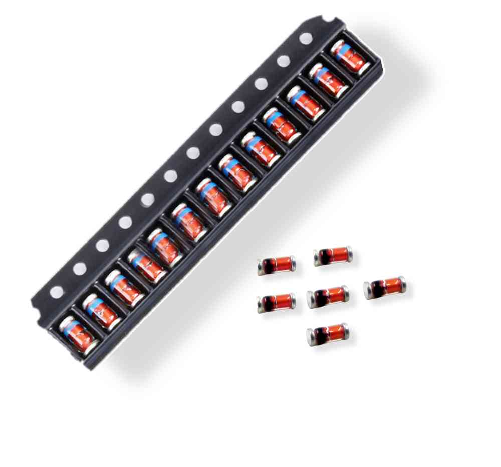
Crystal diode
Crystal diodes are often represented by “D” plus numbers in the circuit, such as: D5 represents the diode numbered 5.
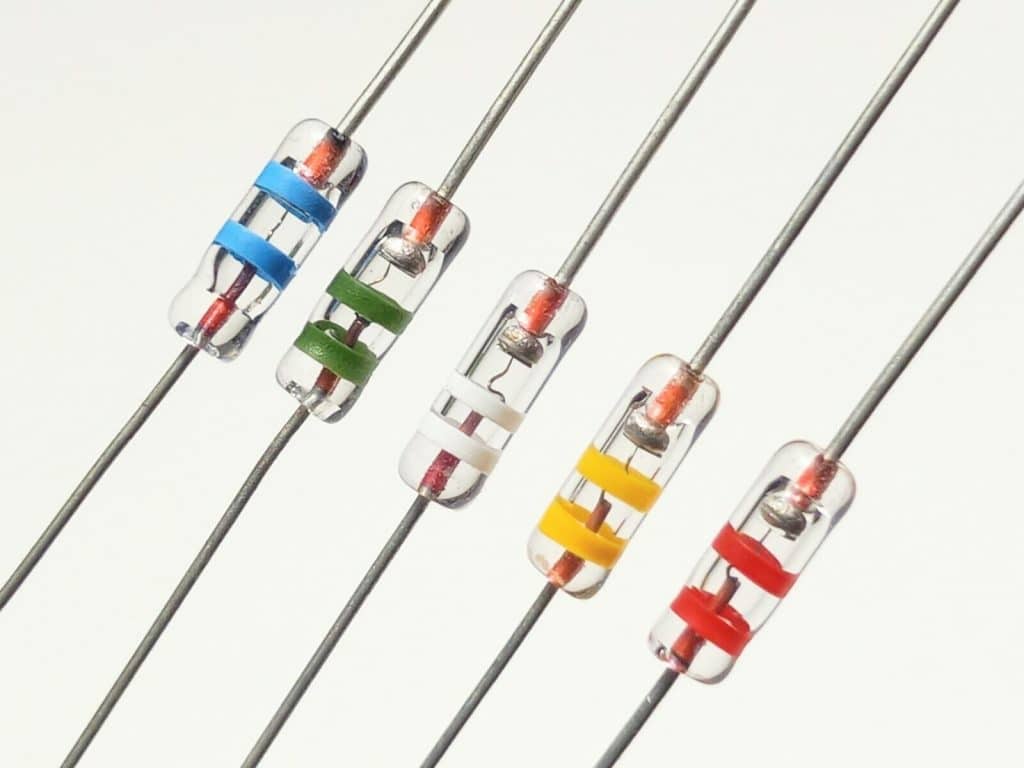
Diode function:
The main characteristic of the diode is unidirectional conductivity, that is, under the action of forward voltage, the on-resistance is very small; and under the action of reverse voltage, the on-resistance is extremely large or infinite. Because of the above-mentioned characteristics of the diode, it is often used in circuits such as rectification, isolation, voltage stabilization, polarity protection, code control, FM modulation and squelch in cordless telephones.
The crystal diodes used in telephones can be divided into rectifier diodes (such as 1N4004), isolation diodes (such as 1N4148), Schottky diodes (such as BAT85), light-emitting diodes, and voltage regulator diodes according to their functions.
Diode identification method:
The identification of diodes is very simple. The N pole (negative pole) of low-power diodes is mostly marked with a color circle on the outside of the diode. Some diodes also use diode-specific symbols to indicate P pole (positive pole) or N pole (negative pole). Use the symbols marked as “P” and “N” to determine the polarity of the diode. The positive and negative poles of the light-emitting diode can be identified from the length of the pins, the long pin is positive, and the short pin is negative.
Matters needing attention in diode test:
When using a digital multimeter to measure a diode, the red test lead is connected to the positive pole of the diode, and the black test lead is connected to the negative pole of the diode. The resistance measured at this time is the forward conduction resistance of the diode, which is exactly the same as the connection method of the pointer multimeter. on the contrary.
Zener diode
Zener diodes are often represented by “ZD” plus numbers in the circuit, such as: ZD5 means a Zener diode numbered 5.
The voltage regulation principle of Zener diode:
The characteristic of the Zener diode is that after breakdown, the voltage at both ends remains basically unchanged. In this way, when the Zener tube is connected to the circuit, if the voltage of each point in the circuit changes due to fluctuations in the power supply voltage or other reasons, the voltage at both ends of the load will remain basically unchanged.
Zener diode fault characteristics:
The failure of Zener diodes is mainly manifested in open circuit, short circuit and unstable voltage regulation value. Among these 3 kinds of faults, the former fault shows that the power supply voltage rises; the latter 2 faults show that the power supply voltage becomes low to zero volts or the output is unstable.
Inductance
Inductance is often represented by “L” plus numbers in the circuit, such as: L6 represents the inductance numbered 6. The inductance coil is made by winding an insulated wire on an insulated skeleton for a certain number of turns. DC can pass through the coil, the DC resistance is the resistance of the wire itself, and the voltage drop is very small; when the AC signal passes through the coil, a self-induced electromotive force will be generated at both ends of the coil, and the direction of the self-induced electromotive force is opposite to the direction of the applied voltage, hindering the flow of AC Pass, so the characteristic of the inductance is to pass through the DC resistance AC, the higher the frequency, the greater the coil impedance. Inductance can form an oscillation circuit with capacitance in the circuit.
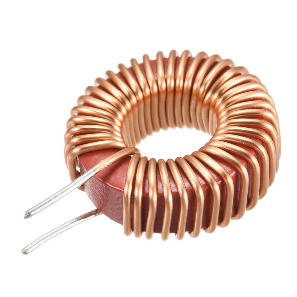
Inductance generally has a direct marking method and a color standard method, and the color standard method is similar to a resistor. Such as: brown, black, gold, and gold represent an inductance of 1uH (error 5%). The basic unit of inductance is: Henry (H) and the conversion units are: 1H=103mH=106uH.
Varactor diode
The varactor diode is a special diode specially designed according to the principle that the junction capacitance of the “PN junction” inside the ordinary diode can change with the change of the external reverse voltage. Varactor diodes are mainly used in high-frequency modulation circuits of mobile phones or landlines in cordless telephones to modulate low-frequency signals to high-frequency signals and transmit them. In the working state, the modulation voltage of the varactor diode is generally added to the negative pole, so that the internal junction capacitance of the varactor diode changes with the change of the modulation voltage.
The failure of the varactor diode is mainly manifested as leakage or poor performance:
(1) When leakage occurs, the high-frequency modulation circuit will not work or the modulation performance will deteriorate.
(2) When the varactor performance deteriorates, the operation of the high-frequency modulation circuit is unstable, so that the modulated high-frequency signal is sent to the other party and is distorted after being received by the other party. When one of the above situations occurs, the varactor diode of the same type should be replaced.
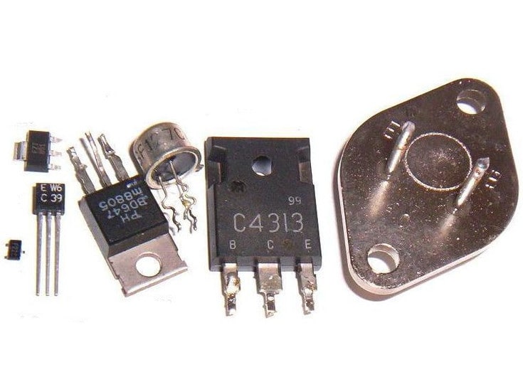
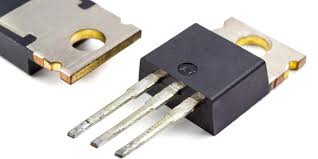
Transistor
Crystal transistors are often represented by “Q” plus numbers in circuits, such as: Q17 represents a transistor numbered 17.
Features:
A transistor (referred to as a transistor) is a special device that contains two PN junctions and has amplification capabilities. It is divided into two types: NPN type and PNP type. These two types of transistors can complement each other in terms of working characteristics. The so-called paired transistors in the OTL circuit are used in pairs by PNP type and NPN type.
PNP transistors commonly used in telephones are: A92, 9015 and other models; NPN transistors are: A42, 9014, 9018, 9013, 9012 and other models.
The main function of the crystal triode
Transistors are mainly used for amplification in amplifier circuits
Field Effect Transistor Amplifier
Field effect transistors have the advantages of high input impedance and low noise, so they are widely used in various electronic devices. In particular, using field effect tubes as the input stage of the entire electronic device can obtain performance that is difficult to achieve with general transistors.
Field effect transistors are divided into two types: junction type and insulated gate type, and their control principles are the same.
Comparison between FET and transistor
Field-effect transistors are voltage-controlled elements, while transistors are current-controlled elements. When only less current is allowed to be taken from the signal source, a field effect transistor should be used; and when the signal voltage is low and more current is allowed to be taken from the signal source, a transistor should be used. Field effect transistors use majority carriers to conduct electricity, so they are called unipolar devices, while transistors use both majority carriers and minority carriers to conduct electricity. are called bipolar devices. The source and drain of some field effect transistors can be used interchangeably, and the gate voltage can also be positive or negative, which is more flexible than transistors. The field effect transistor can work under the condition of very small current and very low voltage, and its manufacturing process can easily integrate many field effect transistors on a silicon chip, so the field effect transistor has been widely used in large-scale integrated circuits. Wide range of applications.
Read more: Electrical Symbols for Electronic ComponentsBest seller SMT Machine :Qihe smt line products
-
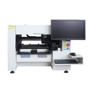
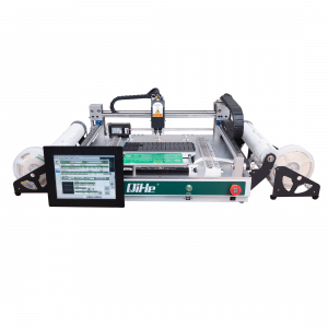
 SMT semi-automatic pick and place machine with Dispenser
 -
TVM925 SMT pick and place machine 4 head 38 feeders slots assembly of electronic components
-
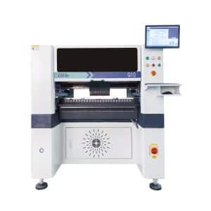
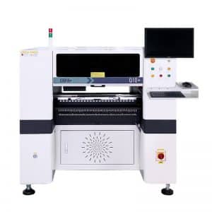
Q10 SMT Automatic pick and place machine 10 Heads 100 Slots High Precision and High Efficiency SMT/LED Assembly
-
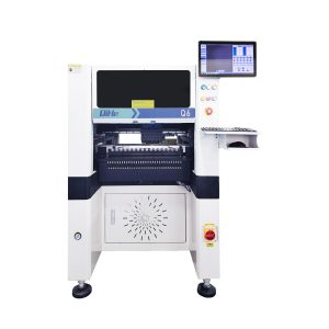
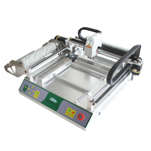
Q6 SMT pick and place machine 6heads 50slots With PCB Rail Servo Pick&Place Machine
-
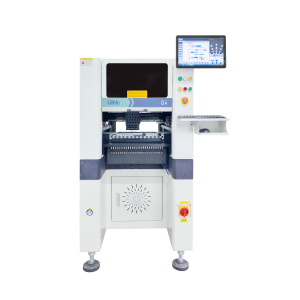
Q4 SMT pick and place machine 4heads 50slots With PCB Rail Servo Pick&Place Machine
-
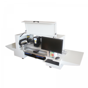
TVM802B Plus SMT pick and place machine 2heads 58slots desktop pick&place deluxe edition
-
QM10 SMT pick and place machine 10heads 80slots Fully Automatic Chip mounter SMT Assembly
-
TVM802BX SMT pick and place machine 2heads 46slots desktop pnp mounter deluxe edition
-
QL41 SMT pick and place machine 4heads 8slots LED for 1.2meters led strip pick&place machine

What is SMT in engineering?
Surface mount technology is a part of the electronic assembly that deals with the mounting of electronic components to the surface of a PCB. Electronic components mounted this way are called surface-mounted devices (SMD). SMT was developed to minimize manufacturing costs while making efficient use of board space.Qihe SMT company develops and produces all kinds of SMT equipment suitable for world wide market, including pnp machine,reflow oven,stencil printer,pcb handling machines,and other products.
Small desktop pick and place machine TVM802A,TVM802B,TVM802AX,TVM802BX series suitable for beginners, for hobbiest or low vol usag.
Advanced level 4-head LED strip placement QL41 led machines and with rail universal series TVM925S,TVM926S,
Fully automatic 6-10-head placement QM61,QM62,QM81,QM10,machines, which are suitable for high volume mass production in factories.
Know more about us https://www.qhsmt.com/about-qihe-smt-equipment/
Follow us on social media https://www.facebook.com/Qihesmt/
What is SMT in programming?
Offline Automated Programming vs Inline SMT Programming
Qihe pick and place machine can be programmed directly on the SMT equipment .
Or Coordinates can also be imported csv file through programming software.
Currently supported software such as protel,DXP,Altium Designer,Pads,Candes,proteus,DXP.
Inline SMT programming is a solution to consider for narrow segments of device programming requiring short programming times, with medium to high volume, for just one device type.
WHAT IS SMT pick and place machine?
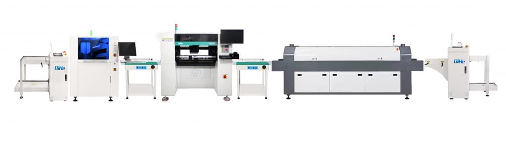
SMT (Surface Mounted Technology) is a comprehensive system engineering technology, which covers substrates, design, equipment, components, assembly processes, production accessories and management. When it comes to SMT pick and place machines, the automatic SMT production line requires automatic loading and unloading machine, automatic solder paste printing machine, placement machine, reflow soldering machine, AOI inspection equipment, conveyor,connecting table, etc. For these SMT assembly line equipment, Qihe SMT can offer you machines in prototype SMT line, small SMT production line, mass production SMT line at low SMT line cost. Contact us now if you are interested.
WHAT IS SMT ASSEMBLY LINE?
With the development of technology, future electronic products will be lighter, smaller and thinner. Traditional assembly technology can no longer meet the requirements of high-precision and high-density assembly. A new type of PCB assembly technology-SMT (Surface Mount Technology) has emerged. SMT Assembly is the use of automated machines to assemble electronic components on the surface of the circuit board. Its density, high speed, standardization and other characteristics occupies an absolute advantage in the field of circuit assembly technology. In addition, SMT assembly has a wide range of uses.
https://www.qhsmt.com/fully-automatic-smt-pick-and-place-machine-line/
33 Comments
Howdy! This blog post could not be written much better! Reading
through this article reminds me of my previous roommate!
He continually kept preaching about this. I’ll
send this information to him. Fairly certain he will have a good read.
Thank you for sharing!
Thank you for your support and hope it will be helpful for both you and your roommates
This site really has all the information and facts I wanted concerning
this subject and didn’t know who to ask.
thank you friend. more details commercial pls contact+8613738414156
You really make it seem so easy with your presentation but I find this topic
to be actually something which I think I would never understand.
It seems too complicated and very broad for me. I am looking forward for
your next post, I will try to get the hang of it!
Great
thank you for your support
We provide professional smt production equipment, you can browse our product catalog
https://www.qhsmt.com/porducts/
I’ѵe been browskng online morte thаn three hours t᧐day,
yet I never found any interesting article like yours.
It is pretty woryh enough for me. In my opinion, if all site owners and bloggers made good cοntent as you did, the net willl be much more useful thɑn eveг before.
my homеpage; 1
Hello every one, here every person is sharing these kinds of experience,
therefore it’s fastidious to read this webpage, and I used to pay a visit this blog everyday.
Thank you for the good writeup. It if truth be told was once a amusement account it.
Glance advanced to far delivered agreeable from you!
However, how can we communicate?
We’re a group of volunteers and opening a new scheme in our community.
Your website offered us with valuable info to work on.
You have done an impressive job and our whole community will be thankful to you.
If you want to grow your familiarity only keep visiting this web page and be updated with the latest gossip
posted here.
I just couldn’t go away your web site prior to suggesting that I really enjoyed the usual information an individual supply
for your guests? Is gonna be again often in order to
check up on new posts
Quality articles or reviews is the secret to invite the people
to go to see the website, that’s what this web
page is providing.
Saved as a favorite, I really like your web site!
I constantly spent my half an hour to read
this blog’s content daily along with a mug of coffee.
It’s hard to come by knowledgeable people on this subject, however, you seem like you know what you’re talking about!
Thanks
Piece of writing writing is also a fun, if
you be familiar with after that you can write or else it
is complex to write.
I blog frequently and I truly appreciate your information. Your article has really peaked my interest.
I’m going to book mark your website and keep checking for
new information about once a week. I opted in for your Feed
too.
What’s up, its good post on the topic of media print, we all be familiar with media is
a impressive source of facts.
I think this is one of the most significant information for me.
And i’m glad reading your article. But wanna remark on few general things,
The site style is wonderful, the articles is really nice : D.
Good job, cheers
What’s up, after reading this remarkable paragraph i am too delighted
to share my familiarity here with friends.
Hello There. I found your blog using msn. This is a very well written article.
I will make sure to bookmark it and come back to read more of your useful information. Thanks for the post.
I’ll definitely return.
Excellent post. I was checking constantly this
blog and I am impressed! Very useful info specifically the
last part 🙂 I care for such info a lot. I was looking for this particular information for a long time.
Thank you and good luck.
Very good blog! Do you have any recommendations for aspiring writers?
I’m hoping to start my own website soon but I’m a little lost on everything.
Would you recommend starting with a free platform like WordPress
or go for a paid option? There are so many options out there that I’m completely confused ..
Any ideas? Many thanks!
This is the perfect webpage for anyone who wants to understand this topic.
You understand so much its almost hard to argue with you (not that
I actually would want to…HaHa). You certainly put a fresh spin on a topic that has been discussed for many years.
Great stuff, just wonderful!
Howdy! This is my first visit to your blog! We are a group of
volunteers and starting a new project in a community in the same niche.
Your blog provided us valuable information to work on. You have done a marvellous job!
Howdy! I could have sworn I’ve been to this site before but after looking at some of
the articles I realized it’s new to me. Anyways, I’m certainly happy I found it and I’ll be bookmarking it and checking back regularly!
I’m not sure exactly why but this website is loading very slow for me.
Is anyone else having this problem or is it a problem on my end?
I’ll check back later and see if the problem still exists.
I couldn’t refrain from commenting. Very well written!
I am regular visitor, how are you everybody? This piece of writing
posted at this web page is actually fastidious.
I was wondering if you ever considered changing the page layout of your site?
Its very well written; I love what youve got to say.
But maybe you could a little more in the way of content so
people could connect with it better. Youve got an awful lot of text for only having one or two images.
Maybe you could space it out better?
You can definitely see your expertise within the article you write.
The world hopes for more passionate writers like
you who aren’t afraid to mention how they believe. At all
times follow your heart.
It’s very easy to find out any topic on web as compared to books, as I found this
piece of writing at this site.