Today author from qihe smt pick and place machine sharing you with The design of PCB single-sided circuit board needs to contact a lot of professional data and some knowledge of physics.
It can be said to be a comprehensive technical project.
To produce high-quality circuit boards,
Not only do you need a solid foundation,
At the same time, it is necessary to maintain sensitivity to resistance
The impedance involved in the PCB board mainly includes the following aspects:
When the direct current of the printed PCB circuit board passes through the wire, there will be a resistance,
This resistance is called resistance, which corresponds to R, and the unit of value is “ohm” (Ω).
The relationship between resistance and current and voltage is: R=V/I
In addition, the resistance is also related to the resistivity (β) of the conductor material,
The length of the wire (L),
The cross-sectional area (S) of the conductor is related.
R=βL/S
a. ResistanceWhen an alternating current flows through a conductor, the resistance encountered is called impedance (Impedance), which corresponds to Z, and the unit is still Ω.
The resistance at this time is different from that encountered by direct current,
In addition to the resistance of the resistor, there is also the resistance of the inductive reactance (XL) and the capacitive reactance (XC).
In order to distinguish the resistance of direct current, the resistance encountered by alternating current is called impedance (Z).
Z=√ R2 + (XL-XC)2
b. Impedance (Z)
In recent years, with the improvement and application of IC integration,
Its signal transmission frequency and speed are getting higher and higher,
Therefore, in the printed circuit board wire, after the signal transmission (emission) reaches a certain value,
will be affected by the printed board wire itself,
This can result in severe distortion or complete loss of the transmitted signal.
This shows that the “thing” that the PCB wire “flows” is not current,
It is the transmission of square wave signals or pulses in energy.
c. Characteristic impedance control (Z0)
The resistance encountered in the transmission of such "signals" as mentioned above,
Also known as “characteristic impedance”, the representative symbol is Z0.
Therefore, it is not enough to solve the problems of “on”, “off” and “short circuit” on the PCB wire.
It is also necessary to control the characteristic impedance of the wire.
That is to say, transmission lines for high-speed transmission and high-frequency signal transmission,
It is much stricter in quality than the transmission wire.
It is no longer acceptable if the “open circuit/short circuit” test is passed, or if the gap or burr does not exceed 20% of the line width.
It must be required to measure the characteristic impedance value, and this impedance should also be controlled within the tolerance.
Otherwise, it can only be scrapped and not reworked.
The characteristic impedance Z0 of the multilayer board signal transmission line,
The current required control range is usually: 50Ω±10%, 75Ω±10%, or 28Ω±10%.
To control the range of variation, four factors must be considered:
(1) Signal line width W;
(2) Signal line thickness T;
(3) The thickness H of the dielectric layer;
(4) Dielectric constant εr.
The greatest influence is the thickness of the medium,
followed by dielectric constant, wire width,
The minimum is the wire thickness.
After selecting the base material, εr changes little, and H changes little,
T is easier to control, but it is difficult to control the line width W within ±10%.
Moreover, the line width problem has problems such as pinholes, gaps, and depressions on the wire.
In a sense, the most effective and most important way to control Z0 is to control and adjust the line width.
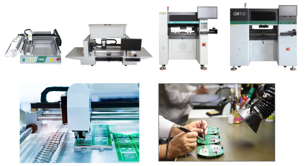
QHSMT is an enterprise specializing in the production of SMT equipment, like pick and place machine ,reflow oven,stencil printer ,smt pick and place machine,pnp,pick&place,pcb assembly,smd chip shooter,pnp machine,chip mounter,smt line,welcome to send inquiry.
Mastering the data of these physical properties will be of great help to PCB design.
Experienced technicians will consider all aspects of factors,
In order to avoid quality problems after most, this is not just relying on experience,
More is a full understanding of the physical properties.
-
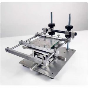
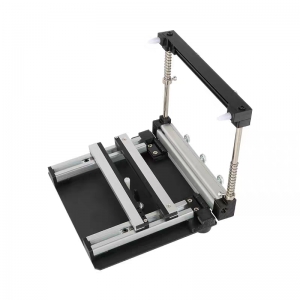
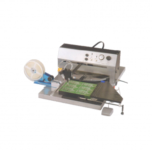
 Benchtop Manual Smt Frameless PCB Solder Paste Stencil Printer Printing Machine
 -
SMT Manual Frameless Pcb Solder Paste Stencil Printer
-
SMT frameless steel stencil screen printing table
-
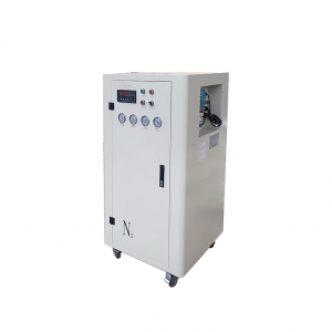
Nitrogen generator, used for selective welding
-
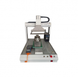
Desktop selection welding QSO-300B
-
Desktop Selective Wave Soldering Machine QH-SHSS341
-
SMT semi-automatic pick and place machine with Dispenser
-
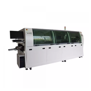
QiHe series wave soldering machine
-
High-speed off-line selective wave soldering QSO-300
WHAT IS SMT ASSEMBLY LINE?
With the development of technology, future electronic products will be lighter, smaller and thinner. Traditional assembly technology can no longer meet the requirements of high-precision and high-density assembly. A new type of PCB assembly technology-SMT (Surface Mount Technology) has emerged. SMT Assembly is the use of automated machines to assemble electronic components on the surface of the circuit board. Its density, high speed, standardization and other characteristics occupies an absolute advantage in the field of circuit assembly technology. In addition, SMT assembly has a wide range of uses.
WHAT IS SMT pick and place machine?
SMT (Surface Mounted Technology) is a comprehensive system engineering technology, which covers substrates, design, equipment, components, assembly processes, production accessories and management. When it comes to SMT pick and place machines, the automatic SMT production line requires automatic loading and unloading machine, automatic solder paste printing machine, placement machine, reflow soldering machine, AOI inspection equipment, connecting table, etc. For these SMT assembly line equipment, Qihe SMT can offer you machines in prototype SMT line, small SMT production line, mass production SMT line at low SMT line cost. Contact us now if you are interested.
WHAT IS SMT PROCESS?
There are mainly three steps in SMT assembly line process flow: solder paste printing, components placement and reflow soldering.
- Solder Paste Printing
Its function in SMT line process is to print the solder-free paste on the pads of the PCB to prepare for the soldering of the components. The equipment used is a screen printing machine, located at the forefront of the SMT production line.
- Components Placement
Its function is to accurately install the surface mount components on the fixed position of the PCB. The equipment used is a placement machine, located behind the screen printing machine in the SMT production line.
- Reflow Soldering
Its function in SMT manufacturing line is to melt the solder paste so that the surface mount components and the PCB board are firmly bonded together. The equipment used is a reflow oven, located behind the placement machine in the fully automatic SMT production line.